By giving compute powers to atomically thin versions of the CMOS sensors now found in most digital cameras, a prototype sensor array can capture images using thousands to millions of times less power, a new study finds.
CMOS sensors are a kind of active pixel sensor, which combine a light detector with one or more transistors. Although scientists have made steady progress toward more energy-efficient light detectors, the signal-conversion and data-transmission capabilities of active pixel sensors are currently extremely energy-inefficient, says study colead author Akhil Dodda, an electronics engineer who was at Penn State University at University Park, in Pennsylvania, at the time of the research.
In the new study, the researchers sought to add in-sensor processing to active pixel sensors to reduce their energy and size. They experimented with the 2D material molybdenum disulfide, which is made of a sheet of molybdenum atoms sandwiched between two layers of sulfur atoms. Using this light-sensitive semiconducting material, they aimed to combine image-capturing sensors and image-processing components in a single device.
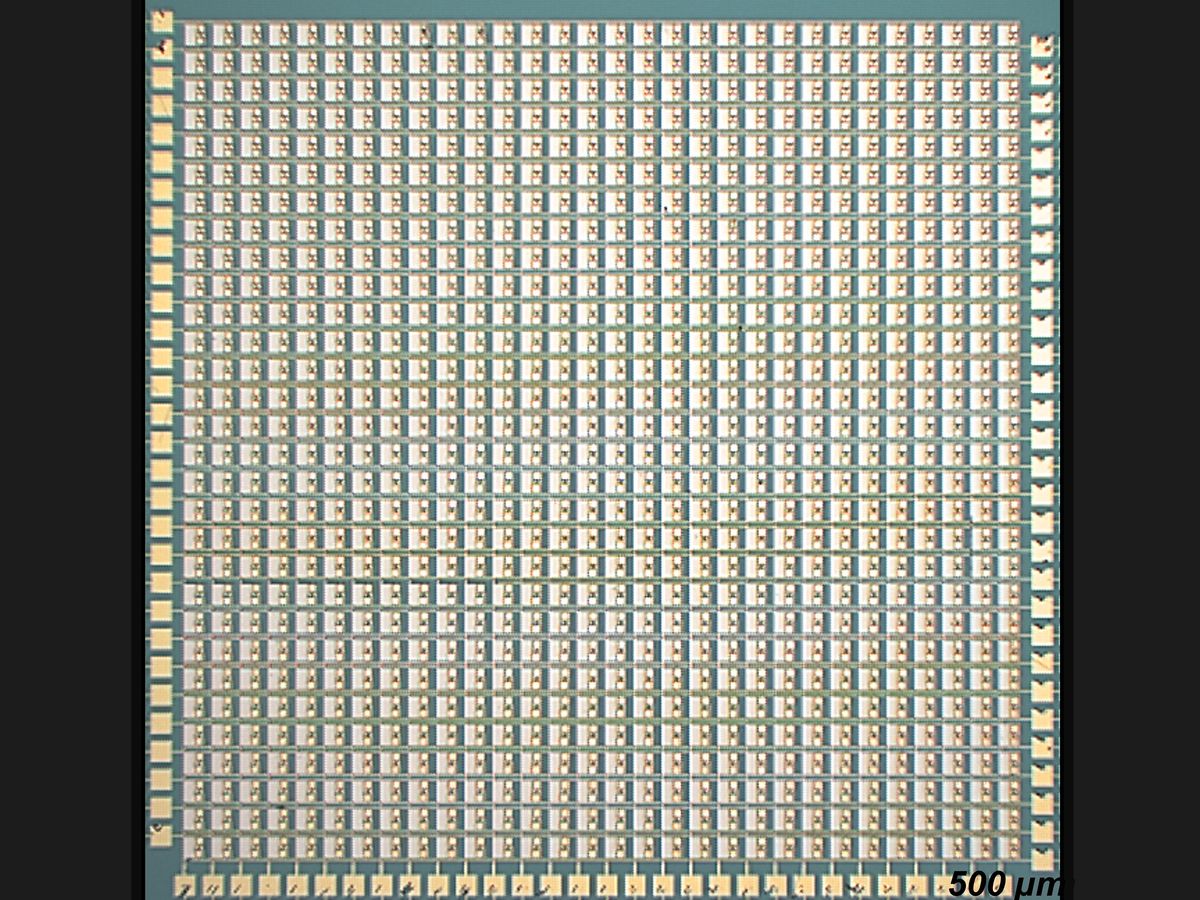
The scientists developed a 2D active pixel sensor array in which each pixel possessed a single programmable phototransistor. These light sensors can each perform their own charge-to-voltage conversion without needing any extra transistors. “We were often surprised by the research outcomes from this nanometer-thick material,” says study colead author Darsith Jayachandran, an electronics engineer at Penn State University at University Park.
The prototype array contained 900 pixels in 9 square millimeters, with each pixel about 100 micrometers large. In comparison, state-of-the-art CMOS sensors from Omnivision and Samsung have reached about 0.56 µm in size. However, commercial CMOS sensors also require additional circuitry to detect low light levels, increasing their overall area, which the new array does not, Dodda says.
In addition, the new device required only a few dozen picowatts—trillionths of a watt—per pixel, Jayachandran says. In comparison, a conventional CMOS sensor might demand roughly thousands to 10 million times more power per pixel, he says.
When compared with commercial germanium sensors, the new devices proved roughly a million times more responsive to light and could detect signals about one-thousandth as strong. They also possessed high dynamic range, and performed in a uniform manner across different wavelengths of light and across the entire array.
The new sensors also possessed the ability to quickly reset in order to help eliminate noise in the images the array captured. The researchers also achieved higher manufacturing yields with this new sensor technology.
“We believe our low-power 2D active pixel sensor platform will be a significant boost when it comes to developing smart cameras in the years to come,” Dodda says. “With this technology, we can enhance the quality of images further with minimal battery consumption.”
A major stumbling block this research faces has resulted in the successful transfer of the 2D phototransistors onto the other electronics that make up the device. Improving the transfer process would help enable “our grand vision of developing a smart, low-power camera,” Jayachandran says.
The scientists detailed their findings 17 November in the journal Nature Materials.
- Samsung and Omnivision Claim Smallest Camera Pixels - IEEE ... ›
- Sony Builds AI Into a CMOS Image Sensor - IEEE Spectrum ›
- Chip Hall of Fame: Photobit PB-100 - IEEE Spectrum ›
Charles Q. Choi is a science reporter who contributes regularly to IEEE Spectrum. He has written for Scientific American, The New York Times, Wired, and Science, among others.


