
Last month, two companies said they have reached the next stage in shrinking the pixels on CMOS camera chips. Both Santa Clara–based Omnivision and South Korea’s Samsung claimed pixels with a pitch of just 0.56 micrometers (measured from the center of one pixel to the center of the next), which is about as large as the wavelength of green light.
Samsung currently produces camera chips with 0.64-micrometer pixels, Omnivision released a 0.61-micrometer sensor in January. Omnivision says a 200-megapixel-resolution image sensor with the new 0.56-micrometer pitch will go to customers later this year, and consumers can expect to find them in their smartphones in 2023. Samsung did not say when its imagers would appear, describing the innovation at IEEE International Solid-States Circuits Conference (ISSCC) in February.
Light enters a CMOS imager pixel via a microlens, then passes through a color filter before striking a silicon photodiode. In the photodiode, the light causes charge to accumulate, which is then sensed and the amount digitized by separate circuits. Making all this smaller leads to a host of potential problems.
For example, small pixels are more subject to cross talk, where light entering at a slight angle to the pixel passes through to its neighbor, reducing contrast. So engineers have to build structures that will block this cross talk. Both companies rely on technology called deep trench isolation for this. That is, each pixel’s silicon is separated from its neighbor by a barrier that runs all the way down through the silicon. At the top of the pixel, where the light enters, they use a comparatively short “fence” of dielectric between the silicon and the pixel’s integrated microlenses.
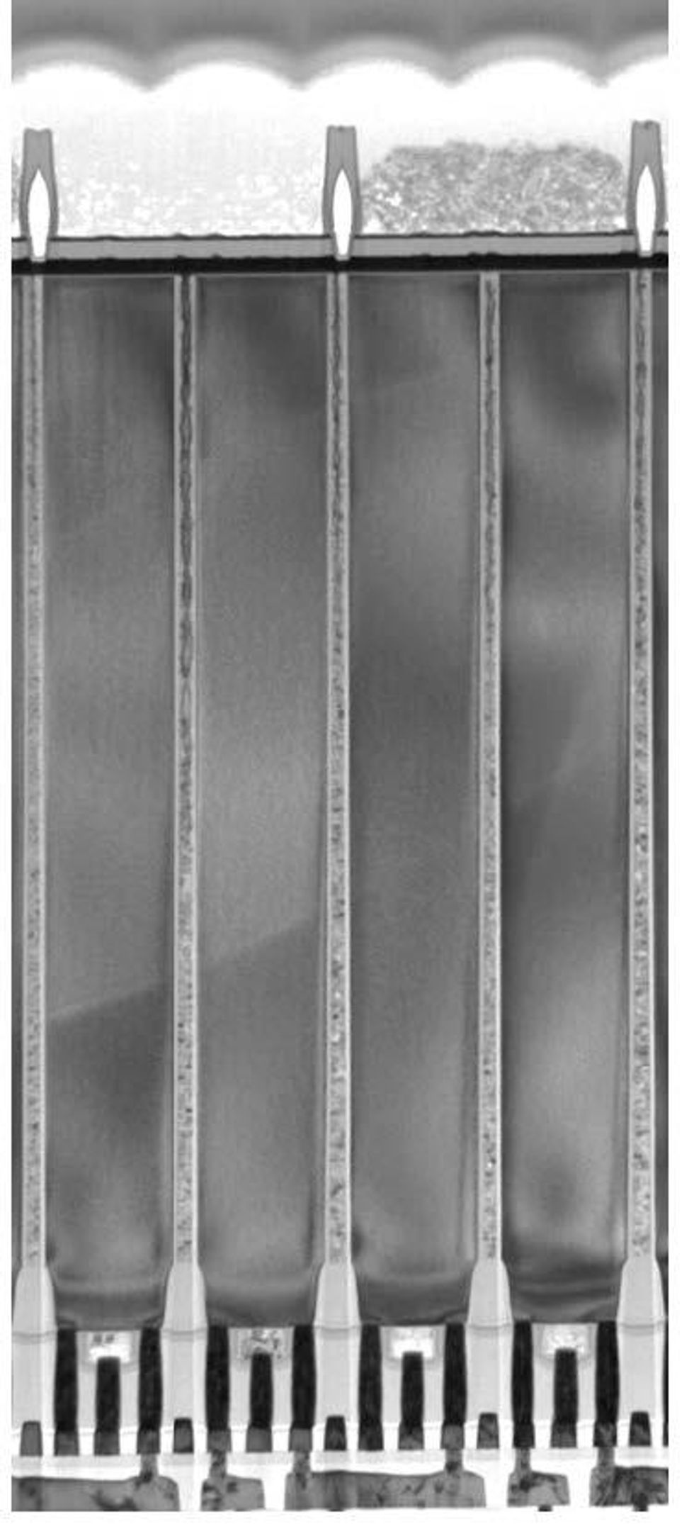 Deep trench isolation structures [long vertical towers] keep light from entering from neighboring pixels. Metal fences [top] also help with this. Samsung boosted the fencing's abilities by inserting a gap of air [bright white] within each.Samsung
Seeking to strengthen the barrier against stray light, Samsung made modifications to the fence. Reasoning that a lower-index-of-refraction material would keep the light out better, Samsung went to the extreme—an air gap. Air has the lowest index of refraction of any material compatible with the CMOS manufacturing process, Samsung’s Sungbong Park told engineers at ISSCC. Through a process of deposition and etching, Samsung engineers made an air cavity within the fence, reducing cross talk by 1.2 percent and boosting quantum efficiency—the ratio of photons converted to electrons—by 7 percent.
Another problem with simply scaling down pixels is that you can store less charge in them before they become saturated, limiting the pixel’s dynamic range. (Dynamic range is the ability to sense in both low and bright light.) Samsung’s 0.64-micrometer device can hold the equivalent of 6,000 electrons, Park said. Shrink that region down to 0.56 micrometers without changing anything and you’re left with only 3,400. Samsung increased the volume by slimming down the isolation walls and adjusting the profile of dopant elements in the photodiode, bringing the capacity back up to 6,000 electrons.
In addition to slimming down the deep trench isolation barrier, Samsung altered its composition. Engineers replaced some of the insulation with material having a higher dielectric constant, making it better at preventing current from flowing when there is no light falling on the pixel.
Both companies also use chip stacking to make more room for pixels. In order to be interpreted by a digital processor, the value at each pixel must first be digitized. At one time, this meant that the photodetecting parts of the pixels all had analog-to-digital converter circuits beside them. But these days, those circuits are built on a separate chip, which is bonded to the photodetector chip, leaving room for more pixels. While Samsung has its own image-chip fabs, Omnivision relied on Taiwan Semiconductor Manufacturing Corp. for both the circuit chip and the photodetector chip.
There will be even tinier pixels in the future, Park assured engineers. Shrinking pixels “is not easy, but we will find a way just as we always have,” he said.
- Mojo Vision Details Low-Power Chips for Augmented Reality ... ›
- Event-Based Camera Chips Are Here, What's Next? - IEEE Spectrum ›
- This MicroLED Display Is Smaller Than a Bug - IEEE Spectrum ›
- New Pixel Sensors Bring Their Own Compute - IEEE Spectrum ›
- Startups Boost Light in Phone Cameras - IEEE Spectrum ›


