A vision for future processors with nearly double the density of transistors is beginning to take shape, now that all three advanced chipmakers have demonstrated CFETS, or complementary field-effect transistors. CFETs are a single structure that stacks both the types of transistors needed for CMOS logic. At the IEEE International Electron Devices Meeting this week in San Francisco, Intel, Samsung, and TSMC showed what progress they’ve made toward the next evolution in transistors.
Chip companies are transitioning from the FinFET device structure in use since 2011 to nanosheet, or gate-all-around, transistors. The names reflect the basic structure of the transistor. In the FinFET, the gate controls the flow of current through a vertical silicon fin. In the nanosheet device, that fin is cut into a set of ribbons, each of which is surrounded by the gate. The CFET essentially takes a taller stack of ribbons and uses half for one device and half for the other. This device, as Intel engineers explained in the December 2022 issue of IEEE Spectrum, builds the two types of transistor—nFETs and pFETs—on top of each other in a single, integrated process.
Experts estimate CFETs to roll out commercially seven to ten years from now, but there is still a lot of work before they are ready.
Intel’s inverter
Intel was earliest of the three to demonstrate the CFET, unveiling an early version at IEDM back in 2020. This time around, Intel is reporting several improvements surrounding the simplest circuit that the CFET makes, an inverter. A CMOS inverter sends the same input voltage to the gates of both devices in the stack and produces an output that is the logical inverse of the input.
“The inverter is done on a single fin,” Marko Radosavljevic, principal engineer at Intel’s components research group, told reporters ahead of the conference. “At maximum scaling, it would be 50 percent” of the size of an ordinary CMOS inverter, he said.
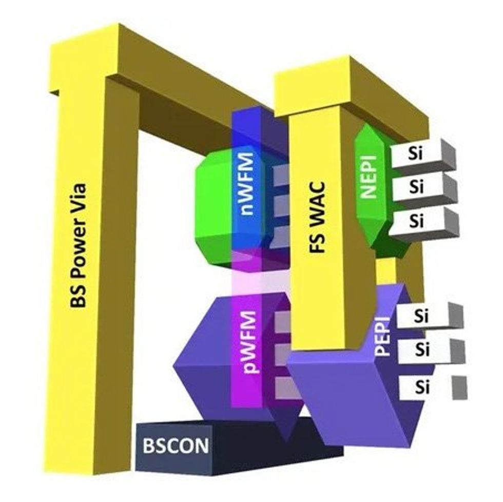 Intel’s inverter circuits depend on a new way of connecting the top and bottom transistors [yellow] and on contacting one of them from beneath the silicon [grey]Intel
The hitch is that squeezing in all the interconnects needed to make that two-transistor stack into an inverter circuit eats away at the area advantage. To keep things tight, Intel tried to remove some of the congestion involved in connecting to the stacked device. In today’s transistors, all the connections come from above the device itself. But later this year, Intel is deploying a technology called backside power delivery that allows interconnects to exist both above and below the surface of the silicon. Using that technology to contact the bottom transistor from below instead of from above significantly simplified the circuit. The resulting inverter had a density quality called contacted poly pitch (CPP, essentially the minimum distance from one transistor gate to the next) of 60 nanometers. Today’s 5 nm node chips have a CPP of about 50 nm.
Additionally, Intel improved the CFET stack’s electrical characteristics by increasing the number of nanosheets per device from two to three, decreasing the separation between the two devices from 50 nm to 30 nm, and using an improved geometry for connecting parts of the device.
Samsung’s secret sauce
Samsung went even smaller than Intel, showing results for 48-nm and 45-nm contacted poly pitch (CPP), compared to Intel’s 60 nm, though these were for individual devices, not complete inverters. Although there was some performance degradation in the smaller of Samsung’s two prototype CFETs, it wasn’t much, and the company’s researchers believe manufacturing process optimization will take care of it.
Crucial to Samsung’s success was the ability to electrically isolate the sources and drains of the stacked pFET and nFET devices. Without adequate isolation, the device, which Samsung calls a 3D stacked FET (3DSFET), will leak current. A key step to achieving that isolation was swapping an etching step involving wet chemicals with a new kind of dry etch. That led to an 80 percent boost in the yield of good devices.
Like Intel, Samsung contacted the bottom of the device from beneath the silicon to save space. However, the Korean chipmaker differed from the American one by using a single nanosheet in each of the paired devices, instead of Intel’s three. According to its researchers, increasing the number of nanosheets will enhance the CFET’s performance.
TSMC takes its shot
Like Samsung, TSMC too managed to get to an industrially-relevant pitch of 48 nm. Its device’s distinctions included a new way to form a dielectric layer between the top and bottom devices to keep them isolated. Nanosheets are generally formed from alternating layers of silicon and silicon germanium. At the appropriate step in the process, a silicon-germanium specific etching method removes that material, releasing the silicon nanowires. For the layer destined to isolate the two device from each other, TSMC used silicon germanium with an unusually high fraction of germanium, knowing that it would etch away faster than the other SiGe layers. That way the isolation layer could be built several steps before releasing the silicon nanowires.
- Meet the Forksheet: Imec’s In-Between Transistor ›
- Intel’s Stacked Nanosheet Transistors Could Be the Next Step in Moore’s Law ›