
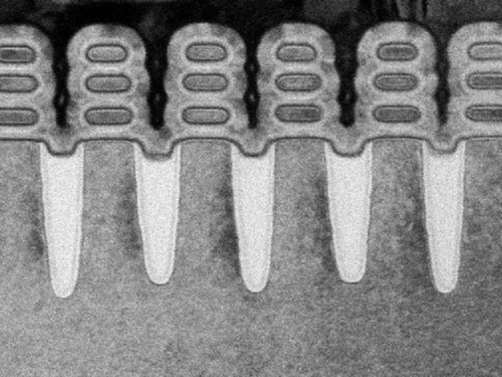
 The Shape of Things to Come: Nanosheet field-effect transistors flow current through multiple stacks of silicon that are completely surrounded by the transistor gate. The design reduces avenues for current to leak through and boosts the amount of current the device can drive.Image: IBM
The modern microprocessor is among the world’s most complex systems, but at its heart is a very simple, and we think beautiful, device: the transistor. There are billions of them in a microprocessor today, and they are nearly all identical. So improving the performance and boosting the density of these transistors is the most straightforward way to make microprocessors—and the computers they power—work better.
That’s the premise behind Moore’s Law, even now that it’s (almost) at an end. You see, making smaller, better transistors for microprocessors is getting more and more difficult, not to mention fantastically expensive. Only Intel, Samsung, and Taiwan Semiconductor Manufacturing Co. (TSMC) are equipped to operate at this frontier of miniaturization. They are all manufacturing integrated circuits at the equivalent of what is called the 7-nanometer node. That name, a vestige of the early days of Moore’s Law, doesn’t have a clear physical meaning anymore, but it nevertheless reflects the degree to which features and devices on an integrated circuit are miniaturized.
Right now, 7 nm is the cutting edge, but Samsung and TSMC announced in April that they were beginning the move to the next node, 5 nm. Samsung had some additional news: It has decided that the kind of transistor the industry had been using for nearly a decade has run its course. For the following node, 3 nm, which should begin limited manufacture around 2020, it is working on a completely new design.
That transistor design goes by a variety of names—gate-all-around, multibridge channel, nanobeam—but in research circles we’ve been calling it the nanosheet. The name isn’t very important. What is important is that this design isn’t just the next transistor for logic chips; it might be the last. There will surely be variations on the theme, but from here on, it’s probably all about nanosheets.
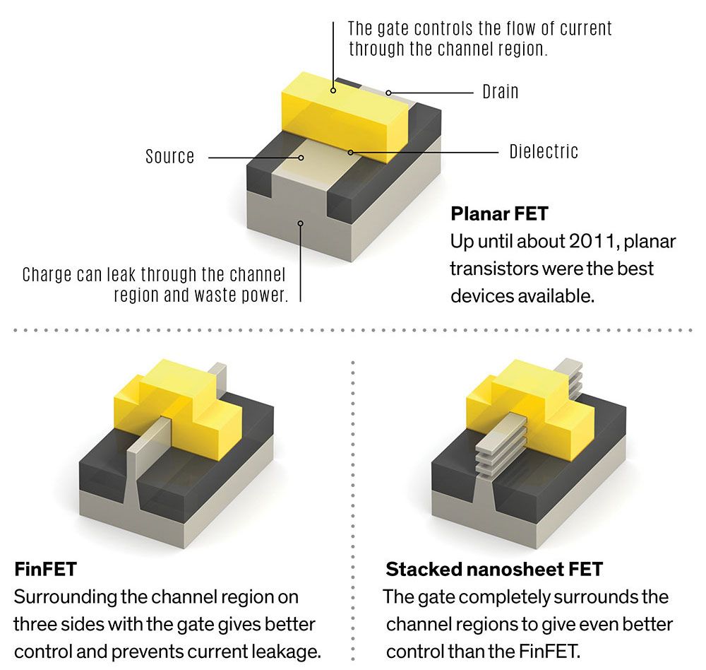
Although the shape and the materials have changed, the metal oxide semiconductor field-effect transistor, or MOSFET—the kind of transistor used in microprocessors—has included the same basic structures since its invention in 1959: the gate stack, the channel region, the source electrode, and the drain electrode. In the device’s original form, the source, drain, and channel are basically regions of silicon that are doped with atoms of other elements to produce either a region with an abundance of mobile negative charge (n-type) or one with an abundance of mobile positive charges (p-type). You need both types of transistors for the CMOS technology that makes up today’s computer chips.
The MOSFET’s gate stack is situated just above the channel region. Today the gate stack is made of metal (for the gate electrode) atop a layer of dielectric material. The combination is designed to project an electric field into the transistor channel region while preventing charge from leaking through.
Applying a large enough voltage to the gate (relative to the source) creates a layer of mobile charge carriers near the interface between the dielectric and the silicon. Once this layer completely bridges the span from source to drain, current can flow across. Reducing gate voltage to near zero should squeeze that conductive pathway shut.
Of course, for current to flow through the channel from the source to the drain, you first need a voltage across it. As transistor structures were made smaller and smaller, the effects of this voltage ultimately led to the biggest shape-shift in transistor history.
That’s because the source-drain voltage can create its own conductive region between the electrodes. As the channel region became shorter and shorter with each new transistor generation, the influence of the drain voltage got bigger. Charge would leak across, ducking beneath the region near the gate. The result was a transistor that was never completely off, wasting power and generating heat.
To stanch the unwanted flow of charge, the channel region had to be made thinner, restricting the path for charge to sneak through. And the gate needed to surround the channel on more sides. Thus, today’s transistor, the FinFET, was born. It’s a design in which the channel region is essentially tilted up on its side to form a slim fin of silicon between the source and the drain, providing a wider path for current to flow through. The gate and dielectric are then draped over the fin, surrounding it on three sides instead of just one.
Evolution of the FET
Since its introduction in 1959, the field-effect transistor has been mostly built into the plane of the silicon. But in order to better control the leakage of current, it took the shape of a protruding fin and will now become stacked sheets.
The FinFET has no doubt been a great success. Though it was invented more than a decade earlier, the FinFET was first commercially introduced in 2011 at the 22-nm node by Intel and later by Samsung, TSMC, and others. Since then it’s been the workhorse of cutting-edge silicon logic in these final stages of Moore’s Law scaling. But all good things come to an end.
With the 3-nm node, FinFETs are not up to the task. The three of us saw this coming in one form or another more than a decade ago, as did others.
Excellent as it is, the FinFET has its problems. For one, it introduced a design limitation that wasn’t a factor for the old “planar” transistor. To see the problem, you have to understand that there’s always a trade-off among a transistor’s speed, power consumption, manufacturing complexity, and cost. And that trade-off has a lot to do with the width of the channel, which is called Weff in device-design circles. More width means you can drive more current and switch a transistor on and off faster. But it also requires a more complicated, costly manufacturing process.
In a planar device, you can make this trade-off simply by adjusting the geometry of the channel. But fins don’t allow as much flexibility. The metal interconnects that link transistors to form circuits are built in layers above the transistors themselves. Because of this, the transistor fins can’t really vary very much in height—equivalent to width in planar designs—without interfering with the interconnect layers. Today, chip designers get around this problem by making individual transistors that have multiple fins.
Another of the FinFET’s shortcomings is that its gate surrounds the rectangular silicon fin on only three sides, leaving the bottom side connected to the body of the silicon. This allows some leakage current to flow when the transistor is off. Many researchers reasoned that to gain ultimate control over the channel region, the gate needed to surround it completely.
Researchers have been taking this idea to its logical conclusion since at least 1990. That year, researchers reported the first silicon device with a gate that completely surrounds the channel region. Since then, a generation of researchers have worked on so-called gate-all-around devices. By 2003, researchers seeking to minimize leakage turned the channel region into a narrow nanowire that bridges the source and the drain and is surrounded by the gate on all sides.
So why don’t gate-all-around nanowires provide the basis for the newest transistor? Again, it’s all about channel width. A narrow wire provides little opportunity for electrons to escape, thus keeping the transistor off when it should be off. But it also provides little room for electrons to flow when the transistor is on, limiting current and slowing switching.
You can get more Weff, and therefore current, by stacking nanowires atop one another. And Samsung engineers unveiled a version of this configuration in 2004, called the multibridge channel FET. But it had several limitations. For one, like the FinFET’s fin, the stack can’t get too high or it will interfere with the interconnect layer. For another, each additional nanowire adds to the device’s capacitance, slowing the transistor’s switching speed. Finally, due to the complexity of making very narrow nanowires, they often wind up being rough around the edges. This surface roughness can impede the speed of charge carriers.
In 2006, engineers working with one of us (Ernst) at CEA-Leti, in France, demonstrated a better idea. Instead of using a stack of nanowires to bridge the source and drain, they used a stack of thin sheets of silicon. The idea was to increase the width of the channel in a smaller transistor, while maintaining tight control over leakage current—and thus provide a better performing, lower-power device. And it works: Under the direction of another of us (Khare), IBM Research took the concept further in 2017, showing that a transistor made from stacked nanosheets actually offered more Weff than a FinFET that takes up the same amount of chip area.
But the nanosheet design offers one more bonus: It restores the flexibility lost in the transition to FinFETs. Sheets can be made wide to boost current or narrow to limit power consumption. IBM Research has made them in stacks of three with sizes ranging from 8 to 50 nm across.
How to Make Nanosheets
Sacrificial layers, selective chemical etchants, and advanced atomically precise deposition technology are needed to make nanosheets.
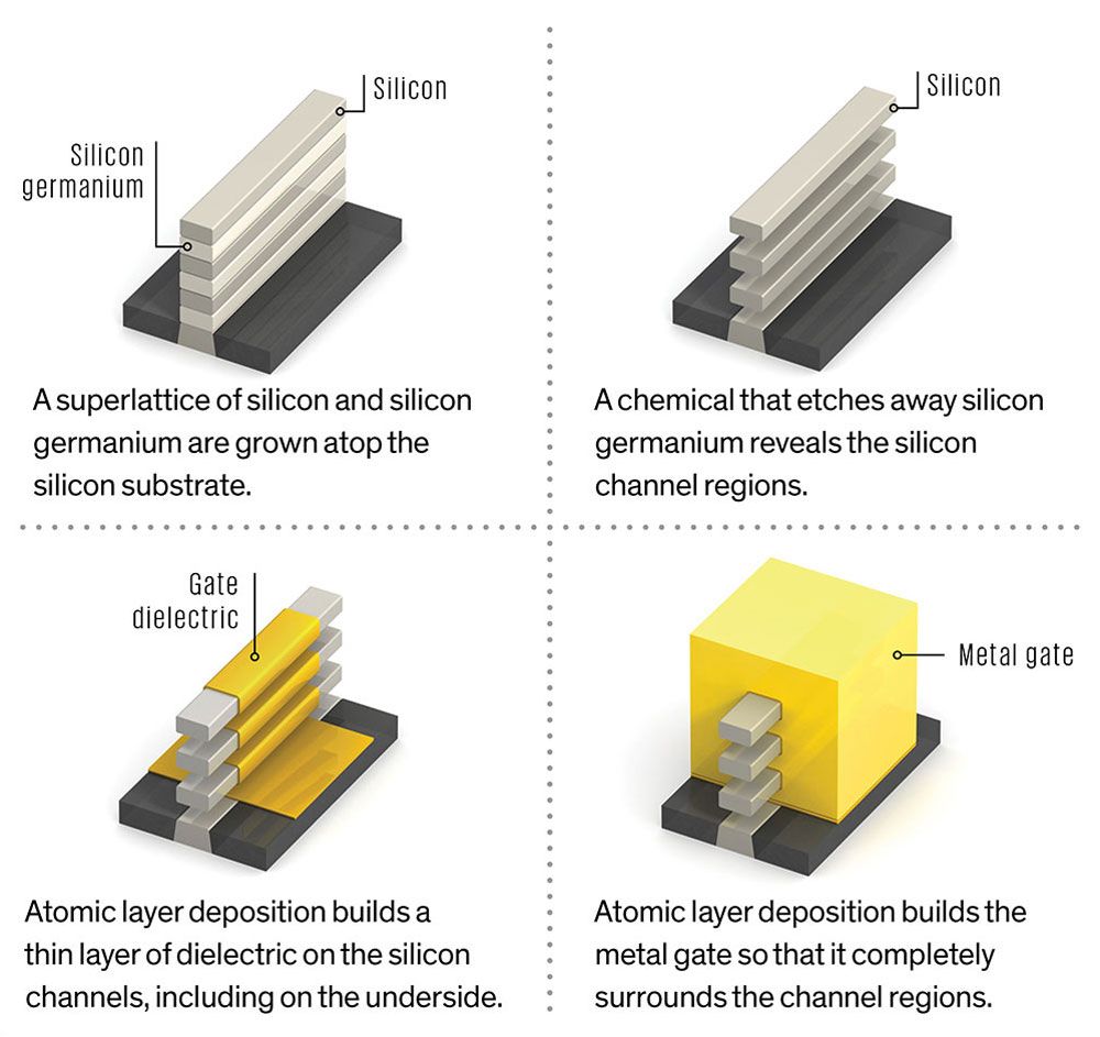
How do you make a nanosheet transistor? It might seem like a tall order, considering that most semiconductor manufacturing processes cut straight down from the top of the silicon or fill straight up from the exposed surface. Nanosheets need to remove material between layers of other material and fill in the gaps with both metal and dielectric.
The main trick is in building what’s called a superlattice—a periodic, layered crystal of two materials. In this case it’s silicon and silicon germanium. Researchers have made superlattices with 19 layers, but the mechanical stresses involved, as well as the capacitances, make using that many layers ill advised. After the appropriate number of layers are grown, we use a chemical that selectively etches silicon germanium but does nothing to silicon, leaving only the silicon nanosheets suspended as bridges between the source and drain. It’s actually not a new idea; engineers at France Telecom and STMicroelectronics used it 20 years ago in experimental “silicon-on-nothing” transistors, devices that tried to limit short-channel effects by burying a layer of air beneath the transistor channel region.
Once you’ve got the silicon nanosheet channel regions constructed, it’s a matter of filling in the gaps, surrounding the channels first with dielectric and then with metal to form the gate stack. Both these steps are done with a process called atomic layer deposition, introduced in semiconductor manufacturing only a little over a decade ago. In this process, a gaseous chemical adsorbs to the chip’s exposed surfaces, even the underside of the nanosheet, to form a single layer. A second chemical is then added, reacting with the first to leave an atomic-scale layer of the needed material, such as the dielectric hafnium-dioxide. The process is so precise that the thickness of the deposited material is controllable down to a single atomic layer.
One of the astounding things about the nanosheet design is that it may extend Moore’s Law so far that it actually outlasts the use of silicon in the channel. To a large degree, what’s at issue here is heat.
Transistor density is still increasing with every technology node. But the amount of heat an IC can reasonably remove—the power density—has been stuck at about 100 watts per square centimeter for a decade. Chipmakers have gone to great lengths to keep from surpassing this fundamental limit. To keep the heat down, clock rates don’t exceed 4 gigahertz. And the processor industry moved to multicore designs, correctly reasoning that several slower processor cores could do the same job as a single fast one while generating less heat. If we ever want to be able to ramp up clock speeds again, we’ll need more energy-efficient transistors than silicon by itself can deliver.
One potential solution is to introduce new materials into the channel region, such as germanium or semiconductors composed of elements from columns III and V of the periodic table, such as gallium arsenide. Electrons can move more than 10 times as fast in some of these semiconductors, allowing transistors made from these materials to switch faster. More important, because the electrons move faster, you can operate the device at a lower voltage, which leads to higher energy efficiency and less heat generation.
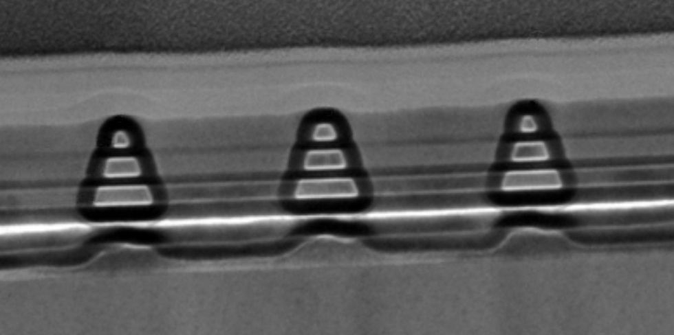 A Nanosheet Forest: Stacked nanosheets also show great promise for compound semiconductors, such as indium gallium arsenide (above), and for silicon alternatives like germanium.Image: Purdue University
In 2012, inspired by earlier work on nanowire transistors and superlattice structures, one of us (Ye) constructed some three-nanosheet devices using indium gallium arsenide, a III-V semiconductor. The results were better than expected. That nanosheet transistor allowed currents of 9,000 microamperes for each micrometer of channel width. That’s about three times better than the best planar InGaAs MOSFETs today. The device performance is still far from the limit of what such transistors could deliver if the manufacturing process were further improved. It’s possible that we can boost the performance by a factor of 10 or more by stacking more nanosheets. (Researchers at HRL Laboratories, in Malibu, Calif., are now working on stacks of tens of nanosheets to develop gallium nitride power devices.) That’s why we believe this strategy is so important to the future of high-speed and energy-efficient integrated circuits.
And InGaAs is not the only option for future nanosheet transistors. Researchers are also exploring other semiconductors with high-mobility charge carriers, such as germanium, indium arsenide, and gallium antimonide. For example, researchers at the National University of Singapore recently constructed a full CMOS IC using a combination of n-type transistors made of indium arsenide and p-type transistors made of gallium antimonide. But a potentially simpler solution is to use doped germanium, because the speeds of electrons and positive charge carriers (holes) traveling through it are both very fast. Germanium still has some manufacturing-process and reliability issues, however. So industry might first take things halfway, using silicon germanium as the channel material.
All in all, stacking nanosheets appears to be the best way possible to construct future transistors. Chipmakers are already confident enough in the technology to put it on their road maps for the very near future. And with the integration of high-mobility semiconductor materials, nanosheet transistors could well carry us as far into the future as anyone can now foresee.
This article appears in the August 2019 print issue as “The Last Silicon Transistor.”
About the Author
Peide Ye is the Richard J. and Mary Jo Schwartz professor of electrical and computer engineering at Purdue University. Thomas Ernst is the scientific director at CEA-Leti in Grenoble, France. Mukesh V. Khare is vice president of semiconductor and AI hardware at IBM Research.