The Conversation (1)

Emily Cooper
LightGreen
Perhaps the most far-reaching technological achievement over the last 50 years has been the steady march toward ever smaller transistors, fitting them more tightly together, and reducing their power consumption. And yet, ever since the two of us started our careers at Intel more than 20 years ago, we’ve been hearing the alarms that the descent into the infinitesimal was about to end. Yet year after year, brilliant new innovations continue to propel the semiconductor industry further.
Along this journey, we engineers had to change the transistor’s architecture as we continued to scale down area and power consumption while boosting performance. The “planar” transistor designs that took us through the last half of the 20th century gave way to 3D fin-shaped devices by the first half of the 2010s. Now, these too have an end date in sight, with a new gate-all-around (GAA) structure rolling into production soon. But we have to look even further ahead because our ability to scale down even this new transistor architecture, which we call RibbonFET, has its limits.
So where will we turn for future scaling? We will continue to look to the third dimension. We’ve created experimental devices that stack atop each other, delivering logic that is 30 to 50 percent smaller. Crucially, the top and bottom devices are of the two complementary types, NMOS and PMOS, that are the foundation of all the logic circuits of the last several decades. We believe this 3D-stacked complementary metal-oxide semiconductor (CMOS), or CFET (complementary field-effect transistor), will be the key to extending Moore’s Law into the next decade.
The Evolution of the Transistor
Continuous innovation is an essential underpinning of Moore’s Law, but each improvement comes with trade-offs. To understand these trade-offs and how they’re leading us inevitably toward 3D-stacked CMOS, you need a bit of background on transistor operation.
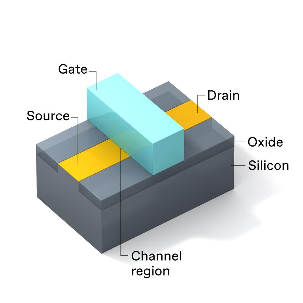
Every metal-oxide-semiconductor field-effect transistor, or MOSFET, has the same set of basic parts: the gate stack, the channel region, the source, and the drain. The source and drain are chemically doped to make them both either rich in mobile electrons ( n-type) or deficient in them (p-type). The channel region has the opposite doping to the source and drain.
In the planar version in use in advanced microprocessors up to 2011, the MOSFET’s gate stack is situated just above the channel region and is designed to project an electric field into the channel region. Applying a large enough voltage to the gate (relative to the source) creates a layer of mobile charge carriers in the channel region that allows current to flow between the source and drain.
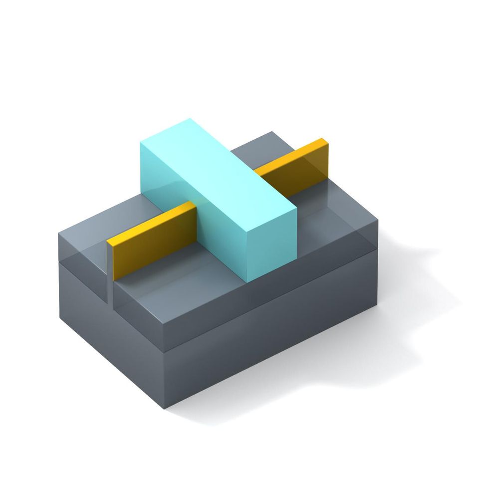
As we scaled down the classic planar transistors, what device physicists call short-channel effects took center stage. Basically, the distance between the source and drain became so small that current would leak across the channel when it wasn’t supposed to, because the gate electrode struggled to deplete the channel of charge carriers. To address this, the industry moved to an entirely different transistor architecture called a FinFET. It wrapped the gate around the channel on three sides to provide better electrostatic control.
Transistor Evolution
Intel introduced its FinFETs in 2011, at the 22-nanometer node, with the third-generation Core processor, and the device architecture has been the workhorse of Moore’s Law ever since. With FinFETs, we could operate at a lower voltage and still have less leakage, reducing power consumption by some 50 percent at the same performance level as the previous-generation planar architecture. FinFETs also switched faster, boosting performance by 37 percent. And because conduction occurs on both vertical sides of the “fin,” the device can drive more current through a given area of silicon than can a planar device, which only conducts along one surface.
However, we did lose something in moving to FinFETs. In planar devices, the width of a transistor was defined by lithography, and therefore it is a highly flexible parameter. But in FinFETs, the transistor width comes in the form of discrete increments—adding one fin at a time–a characteristic often referred to as fin quantization. As flexible as the FinFET may be, fin quantization remains a significant design constraint. The design rules around it and the desire to add more fins to boost performance increase the overall area of logic cells and complicate the stack of interconnects that turn individual transistors into complete logic circuits. It also increases the transistor’s capacitance, thereby sapping some of its switching speed. So, while the FinFET has served us well as the industry’s workhorse, a new, more refined approach is needed. And it’s that approach that led us to the 3D transistors we’re introducing soon.
 In the RibbonFET, the gate wraps around the transistor channel region to enhance control of charge carriers. The new structure also enables better performance and more refined optimization.Emily Cooper
This advance, the RibbonFET, is our first new transistor architecture since the FinFET’s debut 11 years ago. In it, the gate fully surrounds the channel, providing even tighter control of charge carriers within channels that are now formed by nanometer-scale ribbons of silicon. With these nanoribbons (also called nanosheets), we can again vary the width of a transistor as needed using lithography.
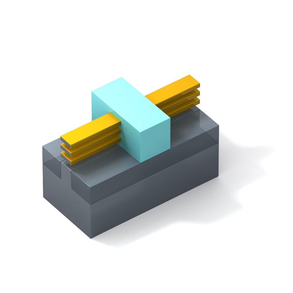
With the quantization constraint removed, we can produce the appropriately sized width for the application. That lets us balance power, performance, and cost. What’s more, with the ribbons stacked and operating in parallel, the device can drive more current, boosting performance without increasing the area of the device.
We see RibbonFETs as the best option for higher performance at reasonable power, and we will be introducing them in 2024 along with other innovations, such as PowerVia, our version of backside power delivery, with the Intel 20A fabrication process.
Stacked CMOS
One commonality of planar, FinFET, and RibbonFET transistors is that they all use CMOS technology, which, as mentioned, consists of n-type (NMOS) and p-type (PMOS) transistors. CMOS logic became mainstream in the 1980s because it draws significantly less current than do the alternative technologies, notably NMOS-only circuits. Less current also led to greater operating frequencies and higher transistor densities.
To date, all CMOS technologies place the standard NMOS and PMOS transistor pair side by side. But in a keynote at the IEEE International Electron Devices Meeting (IEDM) in 2019, we introduced the concept of a 3D-stacked transistor that places the NMOS transistor on top of the PMOS transistor. The following year, at IEDM 2020, we presented the design for the first logic circuit using this 3D technique, an inverter. Combined with appropriate interconnects, the 3D-stacked CMOS approach effectively cuts the inverter footprint in half, doubling the area density and further pushing the limits of Moore’s Law.
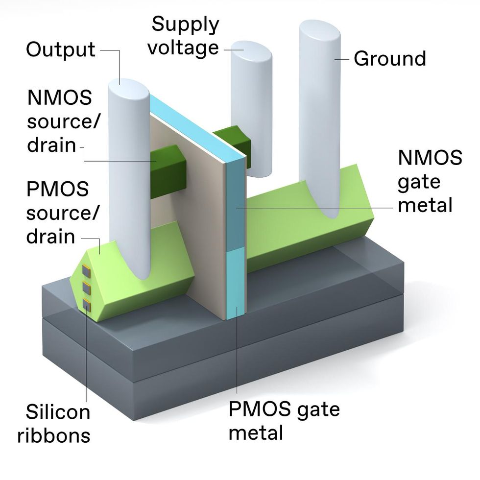
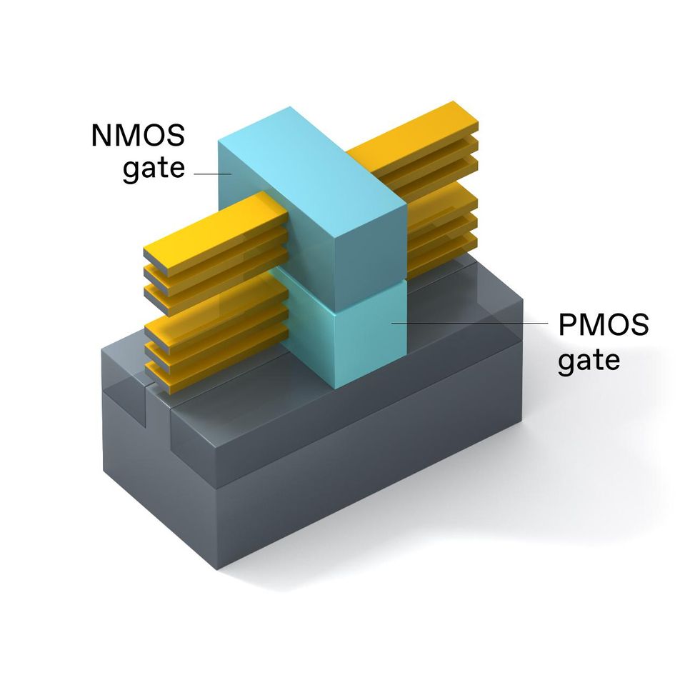 3D-stacked CMOS puts a PMOS device on top of an NMOS device in the same footprint a single RibbonFET would occupy. The NMOS and PMOS gates use different metals.Emily Cooper
Taking advantage of the potential benefits of 3D stacking means solving a number of process integration challenges, some of which will stretch the limits of CMOS fabrication.
We built the 3D-stacked CMOS inverter using what is known as a self-aligned process, in which both transistors are constructed in one manufacturing step. This means constructing both n-type and p-type sources and drains by epitaxy—crystal deposition—and adding different metal gates for the two transistors. By combining the source-drain and dual-metal-gate processes, we are able to create different conductive types of silicon nanoribbons (p-type and n-type) to make up the stacked CMOS transistor pairs. It also allows us to adjust the device’s threshold voltage—the voltage at which a transistor begins to switch—separately for the top and bottom nanoribbons.
In CMOS logic, NMOS and PMOS devices usually sit side by side on chips. An early prototype has NMOS devices stacked on top of PMOS devices, compressing circuit sizes.
Intel
How do we do all that? The self-aligned 3D CMOS fabrication begins with a silicon wafer. On this wafer, we deposit repeating layers of silicon and silicon germanium, a structure called a superlattice. We then use lithographic patterning to cut away parts of the superlattice and leave a finlike structure. The superlattice crystal provides a strong support structure for what comes later.
Next, we deposit a block of “dummy” polycrystalline silicon atop the part of the superlattice where the device gates will go, protecting them from the next step in the procedure. That step, called the vertically stacked dual source/drain process, grows phosphorous-doped silicon on both ends of the top nanoribbons (the future NMOS device) while also selectively growing boron-doped silicon germanium on the bottom nanoribbons (the future PMOS device). After this, we deposit dielectric around the sources and drains to electrically isolate them from one another. The latter step requires that we then polish the wafer down to perfect flatness.
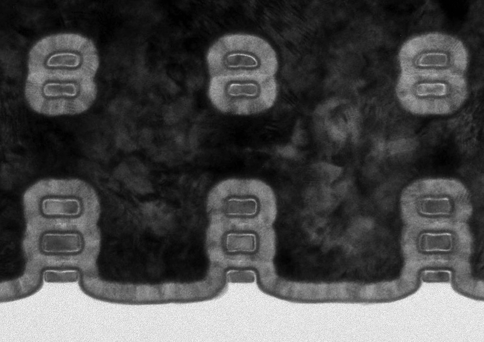
 An edge-on view of the 3D stacked inverter shows how complicated its connections are.Emily Cooper
Finally, we construct the gate. First, we remove that dummy gate we’d put in place earlier, exposing the silicon nanoribbons. We next etch away only the silicon germanium, releasing a stack of parallel silicon nanoribbons, which will be the channel regions of the transistors. We then coat the nanoribbons on all sides with a vanishingly thin layer of an insulator that has a high dielectric constant. The nanoribbon channels are so small and positioned in such a way that we can’t effectively dope them chemically as we would with a planar transistor. Instead, we use a property of the metal gates called the work function to impart the same effect. We surround the bottom nanoribbons with one metal to make a p-doped channel and the top ones with another to form an n-doped channel. Thus, the gate stacks are finished off and the two transistors are complete.
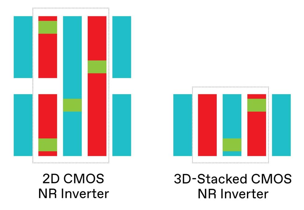 By stacking NMOS on top of PMOS transistors, 3D stacking effectively doubles CMOS transistor density per square millimeter, though the real density depends on the complexity of the logic cell involved. The inverter cells are shown from above indicating source and drain interconnects [red], gate interconnects [blue], and vertical connections [green].Emily Cooper
The process might seem complex, but it’s better than the alternative—a technology called sequential 3D-stacked CMOS. With that method, the NMOS devices and the PMOS devices are built on separate wafers, the two are bonded, and the PMOS layer is transferred to the NMOS wafer. In comparison, the self-aligned 3D process takes fewer manufacturing steps and keeps a tighter rein on manufacturing cost, something we demonstrated in research and reported at IEDM 2019.
Importantly, the self-aligned method also circumvents the problem of misalignment that can occur when bonding two wafers. Still, sequential 3D stacking is being explored to facilitate integration of silicon with nonsilicon channel materials, such as germanium and III-V semiconductor materials. These approaches and materials may become relevant as we look to tightly integrate optoelectronics and other functions on a single chip.
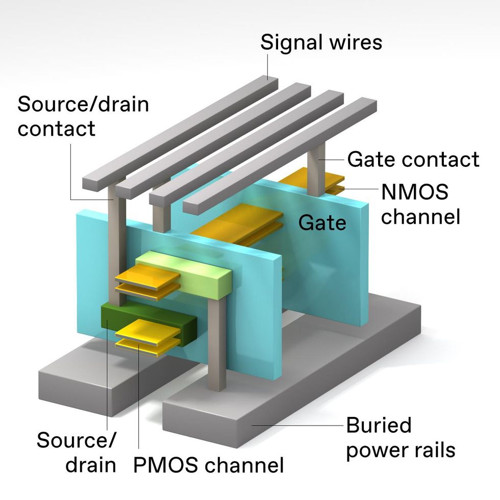
Making all the needed connections to 3D-stacked CMOS is a challenge. Power connections will need to be made from below the device stack. In this design, the NMOS device [top] and PMOS device [bottom] have separate source/drain contacts, but both devices have a gate in common.
Emily CooperThe new self-aligned CMOS process, and the 3D-stacked CMOS it creates, work well and appear to have substantial room for further miniaturization. At this early stage, that’s highly encouraging. Devices having a gate length of 75 nm demonstrated both the low leakage that comes with excellent device scalability and a high on-state current. Another promising sign: We’ve made wafers where the smallest distance between two sets of stacked devices is only 55 nm. While the device performance results we achieved are not records in and of themselves, they do compare well with individual nonstacked control devices built on the same wafer with the same processing.
In parallel with the process integration and experimental work, we have many ongoing theoretical, simulation, and design studies underway looking to provide insight into how best to use 3D CMOS. Through these, we’ve found some of the key considerations in the design of our transistors. Notably, we now know that we need to optimize the vertical spacing between the NMOS and PMOS—if it’s too short it will increase parasitic capacitance, and if it’s too long it will increase the resistance of the interconnects between the two devices. Either extreme results in slower circuits that consume more power.
Many design studies, such as one by TEL Research Center America presented at IEDM 2021, focus on providing all the necessary interconnects in the 3D CMOS’s limited space and doing so without significantly increasing the area of the logic cells they make up. The TEL research showed that there are many opportunities for innovation in finding the best interconnect options. That research also highlights that 3D-stacked CMOS will need to have interconnects both above and below the devices. This scheme, called buried power rails, takes the interconnects that provide power to logic cells but don’t carry data and removes them to the silicon below the transistors. Intel’s PowerVIA technology, which does just that and is scheduled for introduction in 2024, will therefore play a key role in making 3D-stacked CMOS a commercial reality.
The Future of Moore’s Law
With RibbonFETs and 3D CMOS, we have a clear path to extend Moore’s Law beyond 2024. In a 2005 interview in which he was asked to reflect on what became his law, Gordon Moore admitted to being “periodically amazed at how we’re able to make progress. Several times along the way, I thought we reached the end of the line, things taper off, and our creative engineers come up with ways around them.”
With the move to FinFETs, the ensuing optimizations, and now the development of RibbonFETs and eventually 3D-stacked CMOS, supported by the myriad packaging enhancements around them, we’d like to think Mr. Moore will be amazed yet again.

From Your Site Articles
- How the Father of FinFETs Helped Save Moore's Law - IEEE Spectrum ›
- A Better Way to Measure Progress in Semiconductors - IEEE Spectrum ›
- The X-Ray Tech That Reveals Chip Designs - IEEE Spectrum ›
- Meet the Forksheet: Imec’s In-Between Transistor - IEEE Spectrum ›
Related Articles Around the Web
{"imageShortcodeIds":[]}


