The Conversation (0)

Photo: Peter Adams
It was 1995. Advances in chip technology continued apace with Moore’s Law, the observation that the number of transistors on a chip doubles roughly every two years, generally because of the shrinking size of those transistors.
But the horizon no longer seemed limitless. Indeed, for the first time, murmurs throughout the semiconductor industry predicted the death of Moore’s Law. The golden days would be coming to an end, the predictions went, when the size of a critical transistor feature, then around 350 nanometers, reached below 100 nm. Even the U.S. government was worried—so worried that DARPA raised an alarm, launching a program seeking new chip technologies that could extend progress.
Chenming Hu, then a professor of electrical engineering and computer science at the University of California, Berkeley, jumped at the challenge. He immediately thought of a solution—actually, two solutions—and, on a plane ride a few days later, sketched out those designs. One of those ideas, raising the channel through which current flows so that it sticks out above the surface of the chip, became the FinFET, a technology that earned Hu this year’s IEEE Medal of Honor “for a distinguished career of developing and putting into practice semiconductor models, particularly 3-D device structures, that have helped keep Moore’s Law going over many decades.”
The story of the FinFET didn’t begin with Hu putting pencil to paper on an airline tray table, of course.
It started in Taiwan, where Hu was a curious child, conducting stove-top experiments on seawater and dismantling—and reassembling—alarm clocks. As he approached the end of high school, he was still interested in science, mostly chemistry. But instead of targeting a chemistry degree, he applied for the electrical engineering program at the National Taiwan University, even though he didn’t really know what an EE actually did. It was simply a challenge—the electrical engineering program required the highest test scores to get in.
During his last year of college, Hu discovered the industry he would later shake up, thanks to Frank Fang, then a visiting professor from the United States.
“It was 1968,” Hu recalls, “and he told us semiconductors were going to be the material for future televisions, and the televisions would be like photographs we could hang on the wall.”
That, in an era of bulky tube televisions, got Hu’s attention. He decided that semiconductors would be the field for him and applied to graduate programs in the United States. In 1969, he landed at Berkeley, where he joined a research group working on metal-oxide semiconductor (MOS) transistors.
His career soon took a detour because semiconductors, he recalls, just seemed too easy. He switched to researching optical circuits, did his Ph.D. thesis on integrated optics, and went off to MIT to continue his work in that field.
But then came the 1973 oil embargo. “I felt I had to do something,” he said, “something that was useful, important; that wasn’t just writing papers.”
So he switched his efforts toward developing low-cost solar cells for terrestrial applications—at the time, solar cells were used only on satellites. In 1976, he returned to Berkeley, this time as a professor, planning to do research in energy topics, including hybrid cars, an area that transported him back to semiconductors. “Electric cars,” Hu explains, “needed high voltage, high current semiconductor devices.”
Come the early 1980s, that move back to semiconductor research turned out to be a good thing. Government funding for energy research dried up, but a host of San Francisco Bay Area companies were supporting semiconductor research, and transitioning to corporate funding “was not very difficult,” Hu says. He started spending time down in Silicon Valley, not far from Berkeley, invited by companies to teach short courses on semiconductor devices. And in 1982, he spent a sabbatical in the heart of Silicon Valley, at National Semiconductor in Santa Clara.
“Being in industry then ended up having a long influence on me,” Hu says. “In academia, we learn from each other about what is important, so what I thought was interesting really came just because I was reading another paper and felt, ‘Hey, I can do better than that.’ But once I opened my eyes to industry, I found that’s where the interesting problems are.” And that epiphany got Hu looking harder at the 3D structure of transistors.
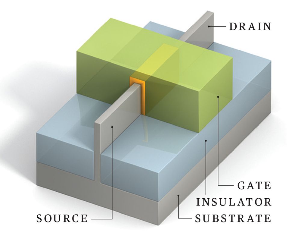 FinFET’s Features: Every transistor has a source, a drain, a conductive channel that connects them, and a gate to control the flow of current down the channel. In a FinFET, raising the channel so that it sticks up above the surface of the chip—like a shark’s fin—allows the gate to wrap around it on three sides, giving the gate greater control.Illustration: Emily Cooper
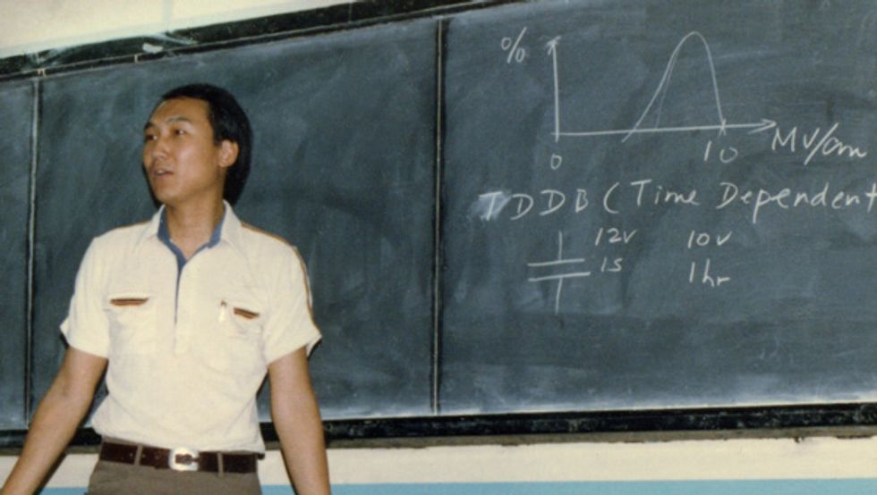
A field-effect transistor has four basic parts—a source, a drain, a conductive channel that connects the two, and a gate to control the flow of current down the channel. As these components were made smaller, people started noticing that the behaviors of transistors were changing with long-term use. These changes weren’t showing up in short-term testing, and companies had difficulty predicting the changes.
In 1983, Hu read a paper published by researchers at IBM that described this challenge. Having spent time at National Semiconductor, he realized the kinds of problems this lack of long-term reliability could cause for the industry. Had he not worked in the trenches, he says, “I wouldn’t have known just how important a problem it was, and so I wouldn’t have been willing to spend nearly 10 years working on it.”
Hu decided to take on the challenge, and with a group of students he developed what he called the hot-carrier-injection theory for predicting the reliability of MOS semiconductors. It’s a quantitative model for how a device degrades as electrons migrate through it. He then turned to investigating another reliability problem: the ways in which oxides break down over time, a rising concern as manufacturers made the oxide layers of semiconductors thinner and thinner.
These research efforts, Hu says, required him to develop a deep understanding of what happens inside transistors, work that evolved into what came to be called the Berkeley Reliability Tool (BERT) and BSIM, a set of transistor models. BSIM became an industry standard and remains in use today; Hu still leads the effort to regularly update its models.
Hu continued to work with his students to study the basic characteristics of transistors—how they work, how they fail, and how they change over time—well into the 1990s. Meanwhile, commercial chips continued to evolve along the path predicted by Moore’s Law. But by the mid-1990s, with the average feature size around 350 nm, the prospects for being able to shrink transistors further had started looking worrisome.
“The end of Moore’s Law was in view,” recalls Lewis Terman, who was at IBM Research at the time.
The main problem was power. As features grew smaller, current that leaked through when a transistor was in its “off” state became a bigger issue. This leakage is so great that it increased—or even dominated—a chip’s power consumption.
“Papers started projecting that Moore’s Law for CMOS would come to an end below 100 nm, because at some point you would dissipate more watts per square centimeter than a rocket nozzle,” Hu recalled. “And the industry declared it a losing battle.”
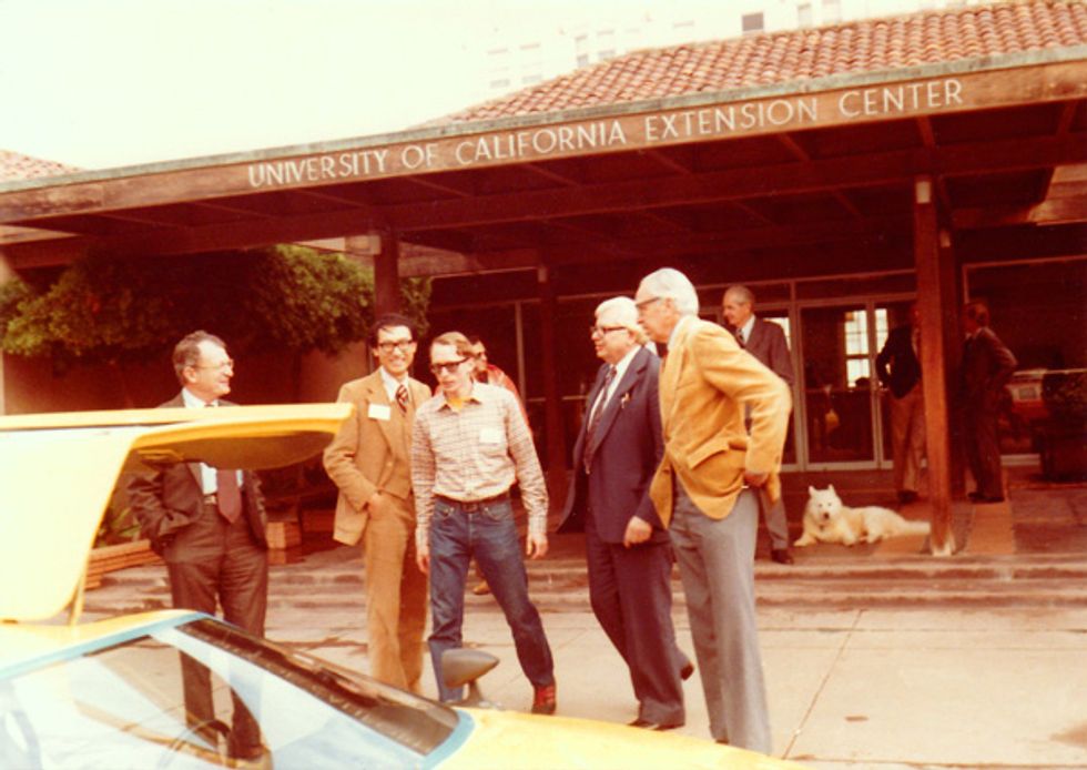
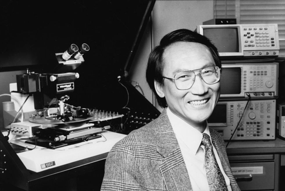 The Road to FinFET: Chenming Hu joined the faculty of the University of California, Berkeley, in 1976 (top). His early research at Berkeley included hybrid cars, like the gas-electric car he presented at the University of California Board of Regents meeting in 1980 (middle). In his lab in 1997 (bottom), Hu was deep in the development of the FinFET, with the help of a DARPA grant.Photos: Chenming Hu
Not ready to give up on Moore’s Law, DARPA (the Defense Advanced Research Projects Agency) looked to fund research that promised to break that barrier, launching an effort in mid-1995 to develop what it called the 25-nm Switch.
“I liked the idea of 25 nm—that it was far enough beyond what the industry thought possible,” Hu says.
Hu saw the fundamental problem as quite clear—making the channel very thin to prevent electrons from sneaking past the gate. To date, solutions had involved thinning the gate’s oxide layer. That gave the gate better control over the channel, reducing leakage current. But Hu’s work in reliability had shown him that this approach was close to a limit: Make the oxide layer sufficiently thin and electrons could jump across it into the silicon substrate, forming yet another source of leakage.
Two other approaches immediately came to mind. One involved making it harder for the charges to sneak around the gate by adding a layer of insulation buried in the silicon beneath the transistor. That design came to be called fully depleted silicon-on-insulator, or FDSOI. The other involved giving the gate greater control over the flow of the charge by extending the thin channel vertically above the substrate, like a shark’s fin, so that the gate could wrap around the channel on three sides instead of just sitting on top. This structure was dubbed the FinFET, which had the additional advantage that using space vertically relieved some of the congestion on the 2D plane, ushering in the era of 3D transistors.
There wasn’t a lot of time to get a proposal submitted to DARPA, however. Hu had heard about the DARPA funding from a fellow Berkeley faculty member, Jeffrey Bokor, who, in turn, had heard about it while windsurfing with a DARPA program director. So Hu quickly met with Bokor and another colleague, Tsu Jae King, and confirmed that the team would pull together a proposal within a week. On a plane trip to Japan a day or two later, he sketched out the two designs, faxing his sketches and a description of his technical approach back to Berkeley when he arrived at his hotel in Japan. The team submitted the proposal, and DARPA later awarded them a four-year research grant.
Ideas similar to FinFET had been described before in theoretical papers. Hu and his team, however, actually built manufacturable devices and showed how the design would make transistors 25 nm and smaller possible. “The others who read the papers didn’t see it as a solution, because it would be hard to build and may or may not work. Even the people who wrote the papers did not pursue it,” says Hu. “I think the difference was that we looked at it and said, we want to do this not because we want to write another paper, or get another grant, but because we want to help the industry. We felt we had to keep [Moore's Law] going.
Chenming Hu
 Photo: Peter Adams
Date of birth: 12 July 1947
Birthplace: Beijing
Height: 5’11”
Family: Wife, Margaret; sons, Raymond and Jason
Education: BS, National Taiwan University, 1968; MS, 1970 and Ph.D., 1973, University of California, Berkeley, all in electrical engineering
First job: Tutor for high school students
First technology job: Assistant professor, MIT
Current job: TSMC Distinguished Professor Emeritus, University of California, Berkeley
Patents: More than 100
Biggest surprise in career: Just how far semiconductor technology has come
Corporate board memberships: ACM Research, Ambarella, Inphi
Hero: Morris Chang
Favorite periodical: Psychology Today
Favorite kind of music: Classical
Favorite movie: Jurassic Park(1993)
Leisure activities: Painting, hiking
Languages spoken: English and Mandarin
Car: Tesla S
Philanthropic Focus: Friends of Children With Special Needs, Fremont, Calif.; Asian Health Services, Oakland, Calif.
Organizational memberships: IEEE, National Academy of Engineering, Chinese Academy of Sciences
Major awards: IEEE Medal of Honor “for a distinguished career of developing and putting into practice semiconductor models, particularly 3-D device structures, that have helped keep Moore’s Law going over many decades,” National Medal of Technology and Innovation from President Barack Obama
“As technologists,” Hu continues, “we have the responsibility to make sure the thing doesn’t stop, because once it stops, we’re losing the biggest hope for us to have more abilities to solve the world’s difficult problems.”
Hu and his team “were well-poised to develop the FinFET because of the way he trains his students to think about devices,” says Elyse Rosenbaum, a former student of his and now a professor at the University of Illinois at Urbana-Champaign. “He emphasizes big picture, qualitative understanding. When studying a semiconductor device, some people focus on creating a model and then numerically solving all the points in its 3D grid. He taught us to step back, to try to visualize where the electric field is distributed in a device, where the potential barriers are located, and how the current flow changes when we change the dimension of a particular feature.”
Hu felt that visualizing the behavior of semiconductor devices was so important, Rosenbaum recalls, that once, struggling to teach his students his process, he “built us a model of the behavior of an MOS transistor using his kids’ Play-Doh.”
“These things looked like a lightning invention,” said Fari Assaderaghi, a former student who is now senior vice president of innovation and advanced technology at NXP Semiconductors. “But his team had been working on fundamental concepts of what an ideal device should be, working from first principles of physics early on; how to build the structure comes from that.”
By 2000, at the end of the four-year grant term, Hu and his team had built working devices and published their research, raising immediate, widespread interest within the industry. It took another decade, however, before chips using FinFETs began rolling off of manufacturing lines, the first from Intel in 2011. Why so long?
“It was not broken yet,” Hu explains, referring to the industry’s ability to make semiconductor circuits more and more compact. “People were thinking it was going to break, but you never fix anything that’s not broken.”
It turned out that the DARPA program managers were prescient—they had called the project the 25-nm Switch, and FinFETs came into play when the semiconductor industry moved to sub-25-nm geometries.
FDSOI, meanwhile, also progressed and is also being used in industry today. In particular, it’s found in optical and RF devices, but FinFETs currently dominate the processor industry. Hu says he never really promoted one approach over the other.
In FinFET’s dormant years, Hu took a three-year break from Berkeley to serve as chief technology officer of semiconductor manufacturer TSMC in Taiwan. He saw that as a chance to pay back the country where he received his initial education. He returned to Berkeley in 2004, continuing his teaching, research in new energy-efficient semiconductor devices, and efforts to support BSIM. In 2009, Hu stopped teaching regular classes, but as a professor emeritus, he still works with graduate students.
Since Hu moved back to Berkeley, FinFET technology has swept the industry. And Moore’s Law did not come to an end at 25 nm, although its demise is still regularly predicted.
“It is going to gradually slow down, but we aren’t going to have a replacement for MOS semiconductors for a hundred years,” Hu says. This does not make him pessimistic, though. “There are still ways of improving circuit density and power consumption and speed, and we can expect the semiconductor industry to keep giving people more and more useful and convenient and portable devices. We just need more creativity and a big dose of confidence.”
This article appears in the May 2020 print issue as “The Father of FinFETs.”
From Your Site Articles


