
There’s a lot of risk in deploying new technology for cutting-edge computer chips. So Intel executives were understandably cautious in executing a plan that next year simultaneously introduces both a new transistor—RibbonFET—and a new way of powering it—PowerVia.
To take some of the risk out of this high-wire act, the company has built and tested processor cores composed of Intel’s current generation of transistors combined with PowerVia. The resulting cores saw more than a 6 percent frequency boost as well as more compact designs and 30 percent less power loss. Just as important, the tests proved that including backside power doesn’t make the chips more costly, less reliable, or more difficult to test for defects. Intel is presenting the details of these tests in Tokyo next week at the IEEE Symposium on VLSI Technology and Circuits.
“We wanted to make sure we could derisk…understand everything about PowerVia, and then go the next step and integrate with RibbonFET,” says Ben Sell, Intel’s vice president of technology development.
PowerVia is Intel’s version of a technology called backside power delivery. Today, chips are constructed with the transistors at the surface of the silicon and all the interconnects that power them and transmit their data signals built above them. Backside power removes all the power-delivering interconnects to beneath the silicon. This has two main effects. First, it leaves more room for the data interconnects above the silicon. And second, the power interconnects can be made larger and therefore less resistive.
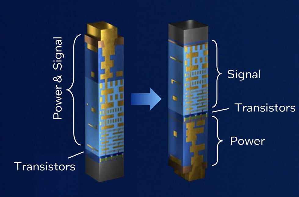 Backside power delivery moves the power interconnects from above the silicon to below it.Intel
That combination improves performance in a few ways. First, with an easier path for power to flow, circuits on the CPU experience less voltage droop; in other words, there is a smaller transient fall in voltage when demand for current increases from, say, a large block of logic switching on. With less droop, transistors can be run faster.
Second, cores can be made more compact, decreasing the length of interconnects between logic cells, which speeds things up. When the standard logic cells that make up the processor core are laid out on the chip, interconnect congestion keeps them from packing together perfectly, leaving loads of blank space between the cells. With less congestion among the data interconnects, the cells fit together more tightly, with some portions up to 95 percent filled. Sell says that’s a double-digit improvement. What’s more, the lack of congestion allowed some of the smallest interconnects to spread out a bit, reducing parasitic capacitance that hinders performance.
The 6 percent gain from these advantages is about half what’s typically delivered when a chipmaker scales down transistors from one technology node to the next. PowerVia delivers it with no change to the transistors.
How PowerVia Is Made
Making PowerVia-enabled chips requires several extra steps and leads to the unusual result that there is hardly any silicon left in the chip. Things start out pretty normal: The transistors, which in this case are FinFETs made using the Intel 4 process, are constructed at the surface of the silicon, as usual. The main difference is that a group of deep, narrow holes are also drilled and then filled in with metal. These nano-TSVs (for through-silicon vias) will be important later. From there, layers of interconnect are formed above the transistors to link them together into logic cells and larger circuits. So far, so regular.
Then the process takes a turn. A blank silicon wafer, called a carrier wafer, is bonded to the top of those interconnects and the whole thing is flipped over. Then the bottom of the original wafer (now on top) is polished away until the ends of the nano-TSVs are exposed. At that point, layers of comparatively chunky interconnects are built up to connect to the nano-TSVs and form the backside power delivery network. These interconnect layers terminate in the bond pads that will link the chip to the package and the rest of the computer.
The resulting chip is thus made up of a large layer of blank silicon for support, a layer of data interconnects, a vanishingly narrow layer of silicon transistors, and a layer of power interconnects.
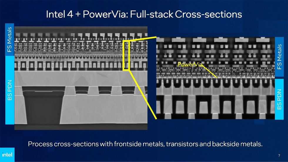 It’s hard to spot the silicon in this PowerVia-enabled processor. (Hint: It’s the bit of white in the middle.) Most of the chip is made up of the signal interconnects above and the much chunkier power interconnects below the transistors. Intel
You might expect that having to build interconnects on both sides of the silicon would make the cost of the chip shoot up. But early on, Intel saw a reason why that would not be the case, says Sell. The smallest, most tightly packed layer of interconnects, called M0, are also the costliest to produce. They can require more than one pass through chipmaking’s most expensive step, extreme ultraviolet lithography. But with no power interconnects to get in the way, the lines in the M0 layer could be six nanometers further apart than they are today. That may not seem like much, but it means it takes less EUV effort to make them. For the process to be introduced next year and for its successor, “the cost savings we get from not scaling so aggressively more than offsets the additional cost from the backside power-delivery process,” Sell says.
Derisking PowerVia
If the plans for PowerVia were going to work, the technology had to meet certain criteria, most of which have to do with not making things worse: Despite existing in a much thinner layer of silicon, the transistors had to work just as well; the power delivery network had to be just as reliable as those built on the front side of the silicon; the heat generated in the silicon couldn’t get out of hand, despite the transistors being sandwiched between interconnect layers; and the ability to debug ICs and spot design defects can’t be hampered.
It took some doing to meet these criteria. For example, the power-interconnect process had to be tweaked to keep from affecting the transistors. And Intel had to set some design rules to keep thermal issues in line. It also had to come up with new methods to make debugging work.
On top of all that, Intel engineers had to ensure that the PowerVia chips’ yield—the fraction of good chips per wafer—was on target to reach high-volume manufacturing, even though these particular chips will never be sold. The goal here was for the yield of Intel 4 PowerVia chips to match those of Intel 4 chips from 9 months ago. PowerVia chips were always going to lag, because any improvements to Intel 4’s yield would take time to translate to the PowerVia experiments. “We did a bit better than that,” says Sell. PowerVia’s yield curve follows Intel 4’s by only 6 months.
2024 and Beyond
With the process for PowerVia worked out, the only change Intel will have to make in order to complete its move from Intel 4 to the next node, called 20A, is to the transistor. RibbonFET, Intel’s take on nanosheet, or gate-all-around, transistors, will then slot in to the already established interconnect scheme.
If all goes well, and Sell says all is going well, the 20A process will be making the company’s Arrow Lake CPUs in 2024. The following technology generation, called 18A, is meant for both Intel products and foundry customers.
Success would put Intel ahead of TSMC and Samsung, in offering both nanosheet transistors and backside power. Samsung has already moved to a gate-all-around device, and it’s unclear when it will integrate backside power. TSMC is scheduled to offer gate-all-around devices in 2025, but it won’t be adding backside power delivery until at least 2026.
- Next-Gen Chips Will Be Powered From Below ›
- Intel’s Take on the Next Wave of Moore’s Law ›
- Intel: Back on Top by 2025? ›
- In 2024, Intel Hopes to Leapfrog Its Chipmaking Competitors - IEEE Spectrum ›
- A Peek at Intel’s Future Foundry Tech - IEEE Spectrum ›


