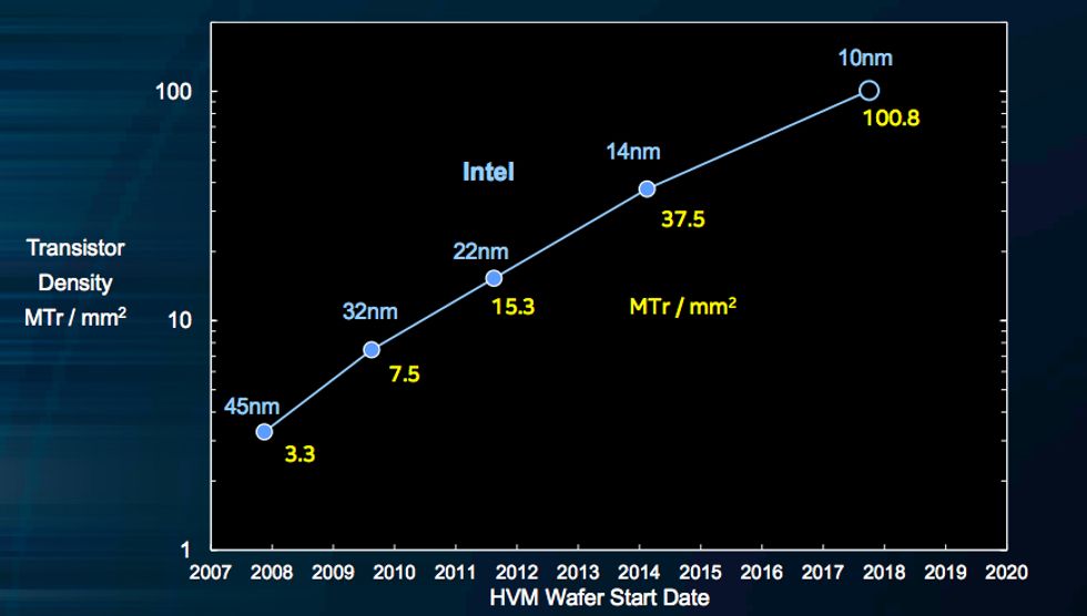
I’ll admit it: journalists like milestones. Nice round numbers and anniversaries make for good headlines. So my ears certainly perked up on Tuesday when Intel said that it can now pack more than 100 million transistors in each square millimeter of chip “for the first time in our industry’s history,” said Kaizad Mistry, a vice president and co-director of logic technology at the company. Delivering more transistors in the same area means the circuitry can be made smaller, saving on cost, or it means that more functionality can be added to a chip without having to make it bigger.
The news came during Intel’s Technology and Manufacturing Day, a behind-the-scenes look at the company’s latest chip classes and packaging technology, and another opportunity for the chipmaker to declare that Moore’s Law is alive and well—at least for Intel.
The nice round 100 million milestone (100.8 million, to be exact) belongs to Intel’s latest-and-greatest chip generation: 10 nanometers. For those uninitiated in semiconductor lingo, the 10 nm designation is a reference to the “node” or manufacturing technology used to make such chips. As a general rule, the smaller the number, the denser the circuitry. But even though node names look like measurements, today the numbers don’t really correspond to the size of any particular feature and there can be significant variation between companies.
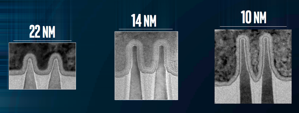
When I wrote about Intel’s 10-nm plans in our January issue previewing the coming year in technology, the company was not yet ready to say much publicly about the specific dimensions of the transistors. This week, they were more forthcoming with figures [pdf]: it’s 34 nm from one fin to the next in the company’s FinFET transistors and 36 nm from one wire to the next in the most dense interconnect layers (down from 42 nm and 52 nm, respectively, in the previous, 14-nm chip generation).
Shorter distances such as these mean that 10nm chips can pack significantly more transistors in a given area. The 100 million density figure comes from a metric that Intel senior fellow Mark Bohr has proposed the industry resurrect, in order to better compare chipmaker offerings. Instead of measuring a chip manufacturing generation by an area taken up by a certain component or set of components, Bohr proposes that we instead measure chip generations by their transistor density—in particular, by the number spit out by an equation that combines the transistor density in a standard 2-input NAND cell and a scan flip-flop logic cell.

And by that metric, Bohr says, Intel has more than doubled its transistor density in recent years. From 22nm to 14nm, the transistor density jumped by a factor of 2.5x. And in the move from 14-nm to 10-nm chip manufacturing technology, the jump was 2.7x, from 37.5 million transistors per square millimeter to more than 100 million. Crucially, the company says, the 10-nm transistors have the capacity for higher speed and greater energy efficiency than their predecessors (although, when I spoke with Bohr late last year, he said the focus lately has been on the latter).
It remains to be seen whether the industry will agree that the new metric is a meaningful one. In comments to EE Times, one analyst said transistor count over a larger area, closer to the size of a real chip, would be a more relevant metric. And an unnamed spokesperson from rival chipmaker TSMC told the site: “I have no idea how Intel does its new calculation...for example, its [first-generation 14nm CPU] Broadwell used to have 18.4 million transistors per mm squared, yet under the new measure it suddenly has 37.5 million transistors per mm2. Are they trying to play paper games?”
Not so fast, says Intel. After this story originally posted, a company representative wrote to IEEE Spectrum to stress the difference between talking about a chip’s transistor density and this metric, which is designed to assess the capabilities of a manufacturing node. “Simply taking the total transistor count of a chip and dividing by its area is not meaningful because of the large number of design decisions that can affect it–factors such as cache sizes and performance targets can cause great variations in this value,” Bohr wrote in his proposal, titled “Let’s Clear Up the Node Naming Mess.”
Even if there is room to quibble over that specific 100 million figure, Intel is also saying that it is more than doubling transistor density with each new chip generation—and that this more aggressive level of miniaturization helps to counteract the slower cadence that has recently set in with respect to the introduction of each new generation. On balance, Intel said, the company is still on a pace that roughly corresponds to a doubling of transistor density every couple of years.
Intel calls the suite of strategies it uses to accomplish this more-than-doubling “hyperscaling.” It includes design improvements, but a big piece is the company’s approach to laying down the patterns that ultimately become the chip’s transistors and wiring, which Intel fellow Ruth Brain outlined in her talk [pdf].
With its 14-nm chips, Brain said, Intel began using a strategy called self-aligned double patterning (SADP). SADP is a form of multiple patterning, a range of strategies that can be used to make chip features much smaller than the 193-nm light that is used to print them by splitting the patterning process into multiple steps.

Other companies, Brain said, use a simple multiple patterning approach that essentially prints the same pattern multiple times, offset slightly. But that technique relies on a lithography machine’s ability to pinpoint the same spot for each exposure, and variability in this process can degrade chip performance and lower the number of usable chips produced. SADP splits up the patterning in a different way, to sidestep this “overlay” issue.
With 10-nm chips, Intel as adopted self-aligned quadruple patterning (SAQP), a similar approach that requires four passes through a lithography machine. Mistry says SAQP has one more generation in it, which would take Intel down to the feature sizes needed to produce the next generation: 7 nm.
Somewhere in there, we may just see extreme ultraviolet (EUV) lithography enter the picture. EUV uses 13.5-nm radiation (pretty much X-rays) instead of 193-nm ultraviolet light for feature patterning.
But back to the present and that 100 million transistors per square millimeter figure. It’s easy to underplay the engineering feats that go into making that sort of milestone (assuming it stands the test of time) possible. “You know one of the remarkable things about Moore’s Law is that Moore’s Law’s past seems preordained and ordinary, and Moore’s Law’s future is difficult and requires inventions,” Mistry told IEEE Spectrum.
Now, he says, the FinFET transistor seems par for the course, but it wasn’t when Intel introduced the technology in 2011. “All these things are difficult, but once they’re done they seem normal,” he adds. “And that’s the magic of Moore’s Law.”
This article was updated on 31 March to add a response from Intel to the comments from TSMC and to correct a caption.
Rachel Courtland, an unabashed astronomy aficionado, is a former senior associate editor at Spectrum. She now works in the editorial department at Nature. At Spectrum, she wrote about a variety of engineering efforts, including the quest for energy-producing fusion at the National Ignition Facility and the hunt for dark matter using an ultraquiet radio receiver. In 2014, she received a Neal Award for her feature on shrinking transistors and how the semiconductor industry talks about the challenge.


