
The 69th Annual IEEE International Electron Device Meeting (IEDM) is set to start on 9 December, and the conference teaser shows that researchers have been extending the road map for a number of technologies, notably those used to make CPUs and GPUs.
Because chip companies can’t keep on increasing transistor density by scaling down chip features in two dimensions, they have moved into the third dimension by stacking chips on top of each other. Now they’re working to build transistors on top of each other within those chips. Next, it appears likely, they will squeeze still more into the third dimension by designing 3D circuits with 2D semiconductors, such as molybdenum disulfide. All of these technologies will likely serve machine learning, an application with an ever-growing appetite for processing power. But other research to be presented at IEDM shows that 3D silicon and 2D semiconductors aren’t the only things that can keep neural networks humming.
3D Chip Stacking
Increasing the number of transistors you can squeeze into a given area by stacking up chips (called chiplets in this case) is both the present and future of silicon. Generally, manufacturers are striving to increase the density of the vertical connections between chips. But there are complications.
One is a change to the placement of a subset of chip interconnects. Beginning as soon as late 2024, chipmakers will start building power-delivery interconnects beneath the silicon, leaving data interconnects above. This scheme, called backside power delivery, has all sorts of consequences that chip companies are working out. It looks like Intel will be talking about backside power’s consequences for 3D devices [see below for more on those]. And Imec will examine the consequences for a design philosophy for 3D chips called system technology cooptimization (STCO). (That’s the idea that future processors will be broken up into their basic functions, each function will be on its own chiplet, those chiplets will each be made with the perfect technology for the job, and then the chiplets will be reassembled into a single system using 3D stacking and other advanced packaging tech.) Meanwhile, TSMC will address a long-standing worry in 3D chip stacking—how to get heat out of the combined chip.
[See the May 2022 issue of IEEE Spectrum for more on 3D chip-stacking technologies, and the September 2021 issue for background on backside power.]
Complementary FETs and 3D Circuits
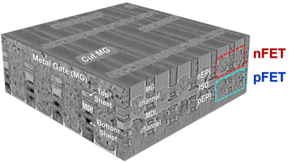
TSMC is detailing a complementary FET (CFET) that stacks an NMOS device on top of a PMOS device.
TSMC
With leading manufacturers of advanced chips moving to some form of nanosheet (or gate-all-around) transistor, research has intensified on the device that will follow—the monolithic complementary field effect transistor, or CFET. This device, as Intel engineers explained in the December 2022 issue of IEEE Spectrum, builds the two flavors of transistor needed for CMOS logic—NMOS and PMOS—on top of each other in a single, integrated process.
At IEDM, TSMC will show off its efforts toward CFETs. They claim improvements in yield, which is the fraction of working devices on a 300-millimeter silicon wafer, and in scaling down the combined device to more practical sizes than previously demonstrated.
Meanwhile, Intel researchers will detail an inverter circuit built from a single CFET. Such circuits could potentially be half the size of their ordinary CMOS cousins. Intel will also explain a new scheme to produce CFETs that have different numbers of nanosheets in their NMOS and PMOS portions.
2D Transistors
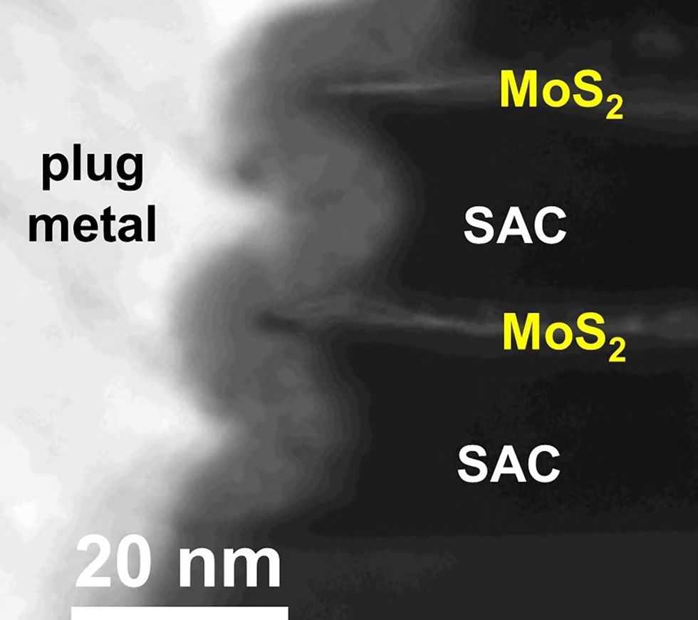
Metal contacts mold around the edge of a 2D semiconductor (MoS2) to create a lower-resistance connection.
TSMC
Scaling down nanosheet transistors (and CFETs, too) will mean ever-thinner ribbons of silicon at the heart of transistors. Eventually, there won’t be enough atoms of silicon to do the job. So researchers are turning to materials that are semiconductors even in a layer that’s just one atom thick.
Three problems have dogged the idea that 2D semiconductors could take over from silicon. One is that it’s been very difficult to produce (or transfer) a defect-free layer of 2D semiconductor. The second is that the resistance between the transistor contacts and the 2D semiconductor has been way too high. And finally, for CMOS you need a semiconductor that can conduct both holes and electrons equally well, but no single 2D semiconductor seems to be good for both. Research to be presented at IEDM addresses all three in one form or another.
TSMC will present research into stacking one ribbon of 2D semiconductor atop another to create the equivalent of a 2D-enabled nanosheet transistor. The performance of the device is unprecedented in 2D research, the researchers say, and one key to the result was a new, wraparound shape for the contacts, which lowered resistance.
TSMC and its collaborators will also present research that manages to produce 2D CMOS. It’s done by growing molybdenum disulfide and tungsten diselenide on separate wafers and then transferring chip-size cutouts of each semiconductor to form the two types of transistors.
Memory Solutions for Machine Learning
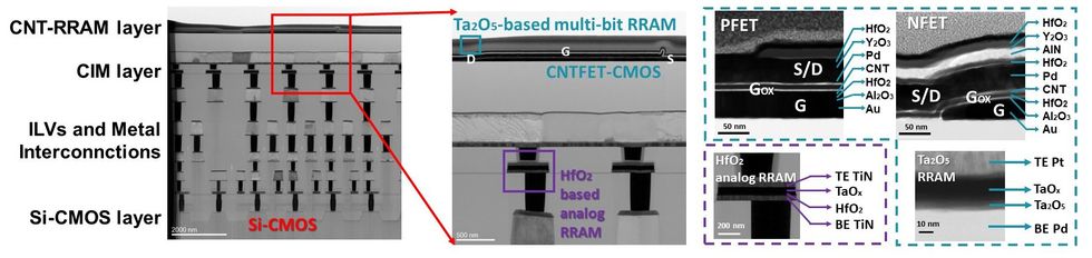
Researchers in China built a machine-learning chip that integrates layers of carbon nanotube transistors, silicon, and memory (RRAM).
Tsinghua University/Peking University
Among the biggest issues in machine learning is the movement of data. The key data involved are the so-called weights and activations that define the strength of the connections between artificial neurons in one layer and the information that those neurons will pass to the next layer. Top GPUs and other AI accelerators prioritize this problem by keeping data as close as they can to the processing elements. Researchers have been working on multiple ways to do this, such as moving some of the computing into the memory itself and stacking memory elements on top of computing logic.
Two cutting-edge examples caught my eye from the IEDM agenda. The first is the use of analog AI for transformer-based language models (ChatGPT and the like). In that scheme, the weights are encoded as conductance values in a resistive memory element (RRAM). The RRAM is an integral part of an analog circuit that performs the key machine-learning calculation, multiply, and accumulate. That computation is done in analog as a simple summation of currents, potentially saving huge amounts of power.
IBM’s Geoff Burr explained analog AI in depth in the December 2021 issue of IEEE Spectrum. At IEDM, he’ll be delivering a design for ways analog AI can tackle transformer models.
Another interesting AI scheme coming up at IEDM originates with researchers at Tsinghua University and Peking University. It’s based on a three-layer system that includes a silicon CMOS logic layer, a carbon nanotube transistor and RRAM layer, and another layer of RRAM made from a different material. This combination, they say, solves a data-transfer bottleneck in many schemes that seek to lower the power and latency of AI by building computing in memory. In tests it performed a standard image-recognition task with the similar accuracy to a GPU but almost 50 times as fast and with about 1/40th the energy.
What’s particularly unusual is the 3D stacking of carbon nanotube transistors with RRAM. It’s a technology the U.S. Defense Advanced Research Projects Agency spent millions of dollars developing into a commercial process at SkyWater Technology Foundry. Max Shulaker and his colleagues explained the plan for the tech in the July 2016 issue of IEEE Spectrum. His team built the first 16-bit programmable nanotube processor with the technology in 2019.
- Intel’s Stacked Nanosheet Transistors Could Be the Next Step in Moore’s Law ›
- Big Trouble in Little Interconnects ›
- 2D Semiconductors Stalk Silicon at the Edge of Moore’s Law ›
- 2D Semiconductors: Shrinking a 2D Transistor With a 1D Wire - IEEE Spectrum ›
- 2D Chip Breakthrough: 6,000 Transistors, 3 Atoms Thick - IEEE Spectrum ›


