The Conversation (2)

Intel; Graphcore; AMD
DarkBlue1
A crop of high-performance processors is showing that the new direction for continuing Moore’s Law is all about up. Each generation of processor needs to perform better than the last, and, at its most basic, that means integrating more logic onto the silicon. But there are two problems: One is that our ability to shrink transistors and the logic and memory blocks they make up is slowing down. The other is that chips have reached their size limits. Photolithography tools can pattern only an area of about 850 square millimeters, which is about the size of a top-of-the-line Nvidia GPU.
For a few years now, developers of systems-on-chips have begun to break up their ever-larger designs into smaller chiplets and link them together inside the same package to effectively increase the silicon area, among other advantages. In CPUs, these links have mostly been so-called 2.5D, where the chiplets are set beside each other and connected using short, dense interconnects. Momentum for this type of integration will likely only grow now that most of the major manufacturers have agreed on a 2.5D chiplet-to-chiplet communications standard.
But to sling truly huge volumes of data around as if it were all on the same chip, you need even shorter and denser connections, and that can be done only by stacking one chip atop another. Connecting two chips face-to-face can mean making thousands of connections per square millimeter.
It’s taken a lot of innovation to get it to work. Engineers had to figure out how to keep heat from one chip in the stack from killing the other, decide what functions should go where and how they should be manufactured, keep the occasional bad chiplet from leading to a lot of costly dud systems, and deal with the resulting added complexities of figuring all that out at once.
Here are three examples, ranging from the reasonably straightforward to the confoundingly complicated, that show where 3D stacking is now:
AMD’s Zen 3
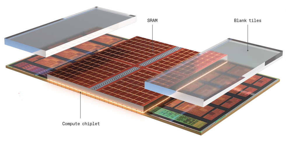
AMD's 3D V-Cache tech attaches a 64-megabyte SRAM cache [red] and two blank structural chiplets to the Zen 3 compute chiplet.
AMD
PCs have long come with the option to add more memory, giving extra-large applications and data-heavy work greater speed. Thanks to 3D chip stacking, AMD’s next-generation CPU chiplet, comes with that option, too. It’s not an aftermarket add on, of course, but if you’re looking to build a computer with some extra oomph, ordering up a processor with an extra-large cache memory could be the way to go.
Even though Zen 2 and the new Zen 3 processor cores are both made using the same Taiwan Semiconductor Manufacturing Corp. manufacturing process—and therefore have the same size transistors, interconnects, and everything else—AMD made so many architectural alterations that even without the extra cache memory, Zen 3 provides a 19 percent performance improvement on average. One of those architectural gems was the inclusion of a set of through-silicon vias (TSVs), vertical interconnects that burrow straight down through most of the silicon. The TSVs are built within the Zen 3’s highest-level cache, blocks of SRAM called L3, which sits in the middle of the compute chiplet and is shared across all eight of its cores.
In processors destined for data-heavy workloads, the Zen 3 wafer’s backside is thinned down until the TSVs are exposed. Then a 64-megabyte SRAM chiplet is bonded to those exposed TSVs using what’s called hybrid bonding—a process that’s like cold-welding the copper together. The result is a dense set of connections that can be as close together as 9 micrometers. Finally, for structural stability and heat conduction, blank silicon chiplets are attached to cover the remainder of the Zen 3 CPU die.
Adding the extra memory by setting it beside the CPU die was not an option, because data would take too long to get to the processor cores. “Despite tripling the L3 [cache] size, 3D V-Cache only added four [clock] cycles of latency—something that could only be achieved through 3D stacking,” John Wuu, AMD senior fellow design engineer, told attendees of the IEEE International Solid State Circuits Conference.
The bigger cache made its mark in high-end games. Using the desktop Ryzen CPU with 3D V-Cache sped games rendered at 1080p by an average of 15 percent. It was good for more serious work as well, shortening the run time for a difficult semiconductor design computations by 66 percent.
The industry’s ability to shrink SRAM is slowing compared to how well it can shrink logic, Wuu pointed out. So you can probably expect future SRAM expansion packs to continue to be made using more established manufacturing processes while the compute chiplets are driven down to Moore’s Law’s bleeding edge.
Graphcore’s Bow AI Processor
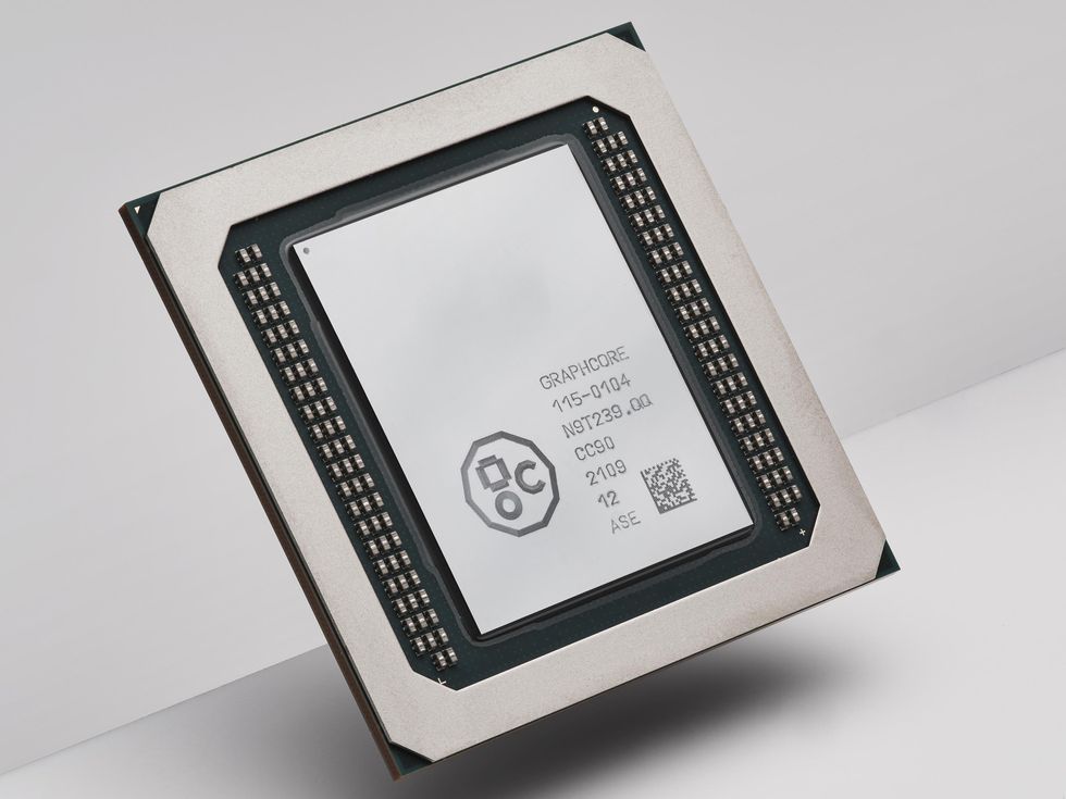
The Graphcore Bow AI accelerator uses 3D chip stacking to boost performance by 40 percent.
Graphcore
3D integration can speed computing even if one chip in the stack doesn’t have a single transistor on it. United Kingdom–based AI computer company Graphcore managed a huge increase to its systems’ performance just by attaching a power-delivery chip to its AI processor. The addition of the power-delivery silicon means the combined chip, called Bow, can run faster—1.85 gigahertz versus 1.35 GHz—and at lower voltage than its predecessor. That translates to computers that train neural nets up to 40 percent faster with as much as 16 percent less energy compared to its previous generation. Importantly, users get this improvement with no change to their software at all.
The power-management die is packed with a combination of capacitors and through-silicon vias. The latter are just to deliver power and data to the processor chip. It’s the capacitors that really make the difference. Like the bit-storing components in DRAM, these capacitors are formed in deep, narrow trenches in the silicon. Because these reservoirs of charge are so close to the processor’s transistors, power delivery is smoothed out, allowing the processor cores to run faster at lower voltage. Without the power-delivery chip, the processor would have to increase its operating voltage above its nominal level to work at 1.85 GHz, consuming a lot more power. With the power chip, it can reach that clock rate and consume less power, too.
The manufacturing process used to make Bow is unique but not likely to stay that way. Most 3D stacking is done by bonding one chiplet to the other while one of them is still on the wafer, called chip-on-wafer [see “AMD’s Zen 3” above]. Instead Bow used TSMC’s wafer-on-wafer, where an entire wafer of one type is bonded to an entire wafer of the other, then diced up into chips. It’s the first chip on the market to use the technology, according to Graphcore, and it led to a higher density of connections between the two dies than could be achieved using a chip-on-wafer process, according to Simon Knowles, Graphcore chief technical officer and cofounder.
Although the power-delivery chiplet has no transistors, those might be coming. Using the technology only for power delivery “is just the first step for us,” says Knowles. “It will go much further than that in the near future.”
[More here]
Intel’s Ponte Vecchio Supercomputer Chip
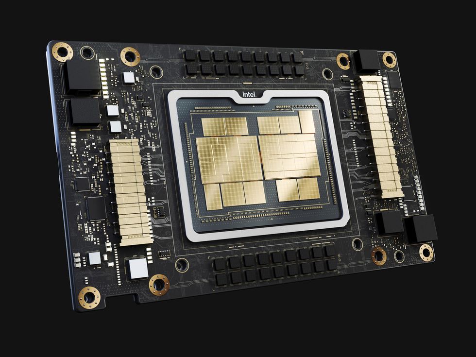
Intel’s Ponte Vecchio processor integrates 47 chiplets into a single processor.
Intel
The Aurora supercomputer is designed to become one of the first U.S.-based high-performance computers (HPCs) to pierce the exaflop barrier—a billion billion high-precision floating-point calculations per second. To get Aurora to those heights, Intel’s Ponte Vecchio packs more than 100 billion transistors across 47 pieces of silicon into a single processor. Using both 2.5D and 3D technologies, Intel squeezed 3,100 square millimeters of silicon—nearly equal to four Nvidia A100 GPUs—into a 2,330-square-millimeter footprint.
Intel Fellow Wilfred Gomes told engineers virtually attending the IEEE International Solid State Circuits Conference that the processor pushed Intel’s 2D and 3D chiplet-integration technologies to the limits.
Each Ponte Vecchio is really two mirror-image sets of chiplets tied together using Intel’s 2.5D integration technology Co-EMIB. Co-EMIB forms a bridge of high-density interconnects between two 3D stacks of chiplets. The bridge itself is a small piece of silicon embedded in a package’s organic substrate. The interconnect lines on silicon can be made twice as densely as those on the organic substrate. Co-EMIB dies also connect high-bandwidth memory and an I/O chiplet to the “base tile,” the largest chiplet upon which the rest are stacked.
The base tile uses Intel’s 3D stacking technology, called Foveros, to stack compute and cache chiplets atop it. The technology makes a dense array of die-to-die vertical connections between two chips. These connections can be 36 micrometers apart from short copper pillars and a microbump of solder. Signals and power get into this stack by means of through-silicon vias, fairly wide vertical interconnects that cut right through the bulk of the silicon.
Eight compute tiles, four cache tiles, and eight blank “thermal” tiles meant to remove heat from the processor are all attached to the base tile. The base itself provides cache memory and a network that allows any compute tile to access any memory.
Needless to say, none of this was easy. It took innovations in yield management, clock circuits, thermal regulation, and power delivery, Gomes said. For example, Intel engineers chose to supply the processor with a higher-than-normal voltage (1.8 volts) so that current would be low enough to simplify the package. Circuits in the base tile reduce the voltage to something closer to 0.7 V for use on the compute tiles, and each compute tile had to have its own power domain in the base tile. Key to this ability were new high-efficiency inductors called coaxial magnetic integrated inductors. Because these are built into the package substrate, the circuit actually snakes back and forth between the base tile and the package before supplying the voltage to the compute tile.
It’s taken 14 years to go from the first petaflop supercomputer in 2008 to exaflops this year, Gomes said. Advanced packaging, such as 3D stacking, is among the technologies that could help shorten the next thousandfold computing improvement to just six years, Gomes told engineers.
[More here]
3D Technologies
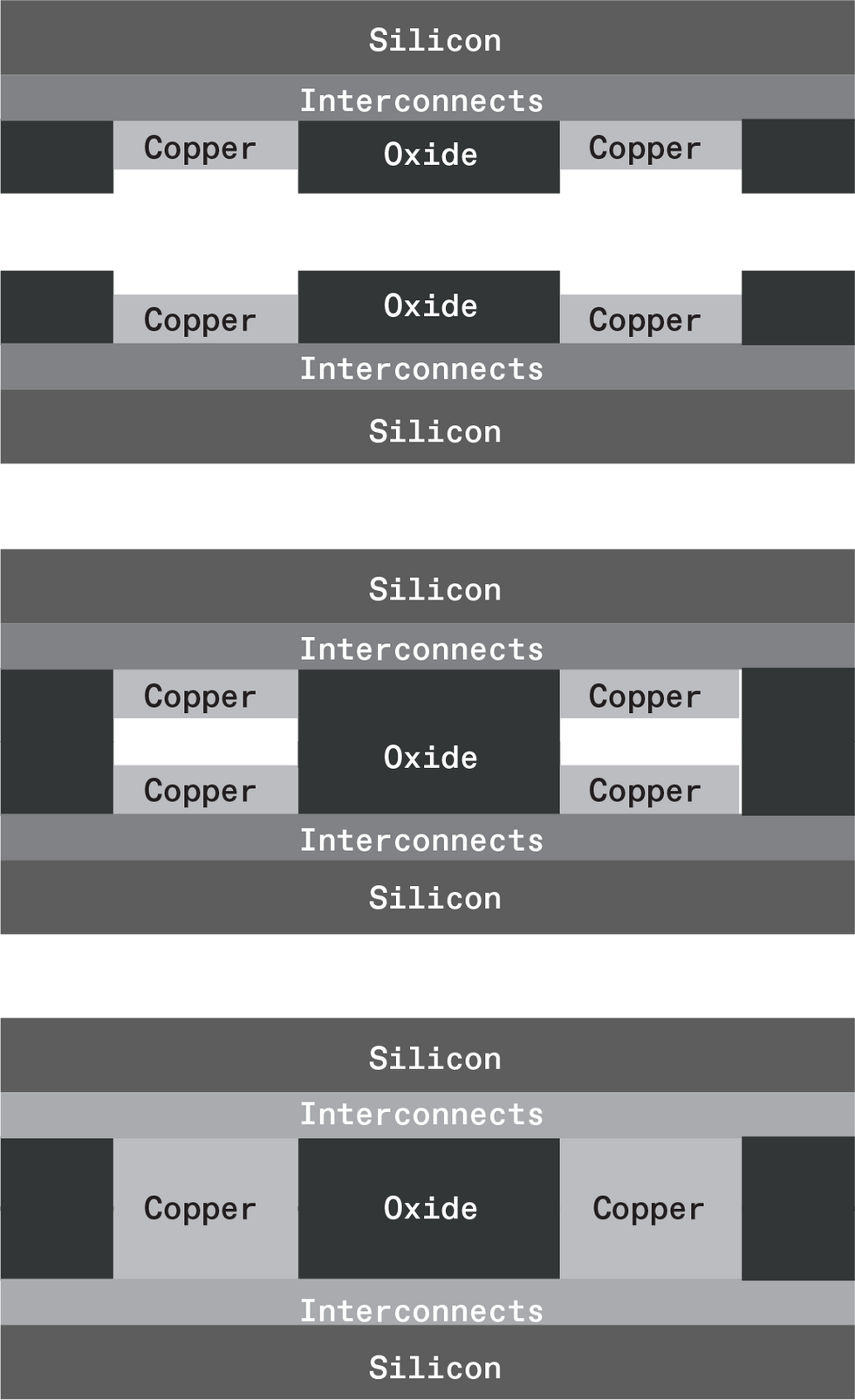
Hybrid bonding starts by forming recessed copper ports at the top “face” of the chip [top]. The surrounding oxide dielectric is chemically activated, so when the two chips are pressed together at room temperature they instantly bond [middle]. The bound chips are annealed, expanding the copper to form a conductive connection [bottom].
Hybrid bonding binds copper pads at the top of a chip’s interconnect stack directly to the copper pads on a different chip. In hybrid bonding, the pads are in small recesses, surrounded by oxide insulator. The insulator is chemically activated and instantly bonds when pressed to its opposite at room temperature. Then, in an annealing step, the copper pads expand and bridge the gap to form a low-impedance link.
Density per millimeter
| 3D microbumps | 3D hybrid bonding |
| 400–1,600 | >10,000 |
Hybrid bonding offers a high density of connections—in the range of 10,000 bonds per square millimeter, many more than in microbump technology, which offers about 400–1,600/mm2 [chart, above]. The pitch—the distance from the edge of one interconnect to the far edge of the next—achievable today is about 9 micrometers, but tighter geometries are in the works. The technology will likely hit its limits around a pitch of 3 µm or so, says Lihong Cao, director of engineering and technical marketing at packaging-technology company ASE Group. The most critical step to improve hybrid bonding is keeping wafers from warping and reducing the surface roughness of each side to nanometer-scale perfection, she says.
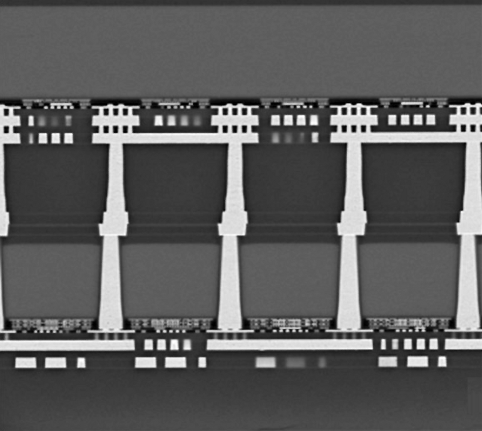
Through-silicon vias [pillars, bottom half] and hybrid bonding [rectangles, center] connect an AMD compute chiplet [bottom] to an SRAM chiplet [top].
Intel
Microbumps are essentially an extremely scaled-down version of a standard packaging technology called flip-chip. In flip-chip, bumps of solder are added to the end points of the interconnects at the top (face) of a chip. The chip is then flipped onto a package substrate with a matching set of interconnects, and the solder is melted to form a bond. To stack two chips with this technology, first one chip must have short copper pillars built so that they protrude from the surface. These are then capped with a “microbump” of solder, and the two chips are joined face-to-face by the melting the solder.
The minimum distance from the start of one connection to the far edge of the next, the pitch, can be less than 50 micrometers when using microbumps. Intel used a 36-µm-pitch version of its Foveros 3D integration technology in the Ponte Vecchio supercomputer chip. Samsung says its microbump technology, called 3D X-Cube, is available with a 30-µm pitch. The technology cannot match hybrid bonding’s density [above]. However, its requirements for alignment and planarization are not as strict as hybrid bonding’s, making it easier to stack multiple chips that are made using different manufacturing technologies onto a single base chip.
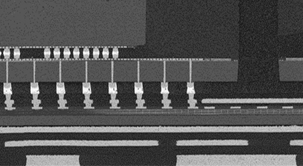
Intel’s Ponte Vecchio uses microbumps [short pillars, top left] to connect a compute chiplet to a base die. Through silicon vias [thin vertical lines, center] send signals from both the base die and the compute tile to the package. The base die connects horizontally to a second base die using a silicon bridge [horizontal bar, right].
Intel
Through silicon-vias (TSVs) are interconnects that descend vertically down through a chip’s silicon. They don’t extend through a wafer’s entire depth, so the backside of the silicon has to be ground away until the TSV is exposed. They are often necessary in 3D stacked chips because the chips are bonded together so that their interconnects are face-to-face. In that case, the TSVs provide the stack with access to power and data. They have been in wide use for years in high-bandwidth dynamic RAM memory, which stacks multiple memory chips vertically. But with 3D chip stacking, the technology has come to logic chips, too.
From Your Site Articles
- The Rise of the Monolithic 3-D Chip - IEEE Spectrum ›
- Graphcore Uses TSMC 3D Chip Tech to Speed AI by 40% - IEEE ... ›
- GlobalFoundries, Arm Close in on 3D Chip Integration - IEEE ... ›
- Linking Chiplets Just Got a Lot Easier - IEEE Spectrum ›
- Keeping Moore’s Law Going is Getting Complicated - IEEE Spectrum ›
- AMD’s Next GPU Is a 3D-Integrated Superchip - IEEE Spectrum ›
- None ›
- Intel Advanced Packaging for Bigger AI Chips - IEEE Spectrum ›
- 3D Heterogeneous Integration Powers New DARPA Fab - IEEE Spectrum ›
Related Articles Around the Web
{"imageShortcodeIds":[]}


