
U.K.-based AI computer company Graphcore made a significant boost to its computers’ performance without changing much of anything about its specialized AI processor cores. The secret was to use TSMC’s wafer-on-wafer 3D integration technology during manufacture to attach a power-delivery chip to Graphcore’s AI processor.
The new combined chip, called Bow, for a district in London, is the first on the market to use wafer-on-wafer bonding, say Graphcore executives. The addition of the power-delivery silicon means Bow can run faster—1.85 gigahertz versus 1.35 GHz—and at lower voltage than its predecessor. That translates to computers that train neural nets up to 40 percent faster with as much as 16 percent less energy compared to its previous generation. Importantly, users get this improvement with no change to their software at all.
“We are entering an era of advanced packaging in which multiple silicon die are going to be assembled together to supplement the performance advantages we can get from increasing progress along an ever-slowing Moore’s Law path,” says Simon Knowles, Graphcore chief technical officer and cofounder. Both Bow and its predecessor the Colossus MK2 were made using the same manufacturing technology, TSMC’s N7.
 Compared with Graphcore’s previous generation, the new computers can train key neural networks about 40 percent faster.Graphcore
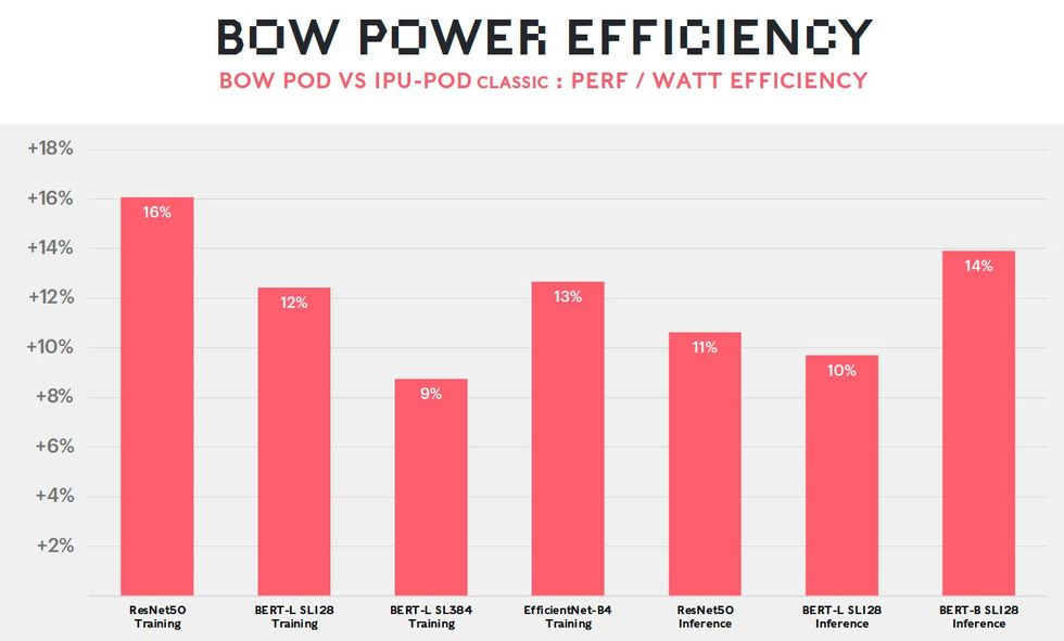 The new systems are up to 16 percent more efficient at training key neural networks.Graphcore
In other 3D-chip-stacking technology, such as Intel’s Foveros, already excised chips are attached to other chips or to wafers. In TSMC’s SoIC WoW technology, two entire wafers of chips are bonded. The chips on each have copper pads that match up when the wafers are aligned. When the two wafers are pressed together, the pads fuse. “You can think of this as a kind of cold weld between the pads,” says Knowles. The top wafer is then thinned down to just a few micrometers and the bonded wafer is diced up into chips.
In Graphcore’s case, one wafer is full of the company’s second generation AI processor (the company calls them IPUs, for intelligence processing units) with 1,472 IPU cores and 900 megabytes of on-chip memory. These processors were already in use in commercial systems and made a good showing in the last round of MLPerf benchmark tests. The other wafer had a corresponding set of power-delivery chips. These chips carry no transistors or other active components. Instead, they are packed with capacitors and vertical connections called through-silicon vias. The latter make power and data connections that pass through the power chip to the processor die.
It’s the capacitors that really make the difference. These components are formed in deep, narrow trenches in the silicon, exactly like the bit-storing capacitors in DRAM. By placing these reservoirs of charge so close to the transistors, power delivery is smoothed out, allowing the IPU cores to run faster at lower voltage. Without the power-delivery chip, the IPU would have to increase its operating voltage above its nominal level to work at 1.85 GHz, consuming a lot more power. With the power chip, it can reach that clock-rate and consume less power, too.
Graphcore executives say wafer-on-wafer technology results in a higher density of connections between the chips than attaching individual chips to a wafer. However, one long-standing concern with this technique was the “known good die” problem. That is, there are always a few chips in a batch of wafers that are flawed. Bonding two wafers would then as much as double the resulting number of flawed chips. Graphcore’s way around this is to let it happen, to a degree. Like some other new AI processors, the IPU is made up of many repeated, and therefore redundant, processor cores and other parts. Any duds can be cut off from the rest of the IPU by means of built-in fuses, says Nigel Toon, Graphcore cofounder and CEO.
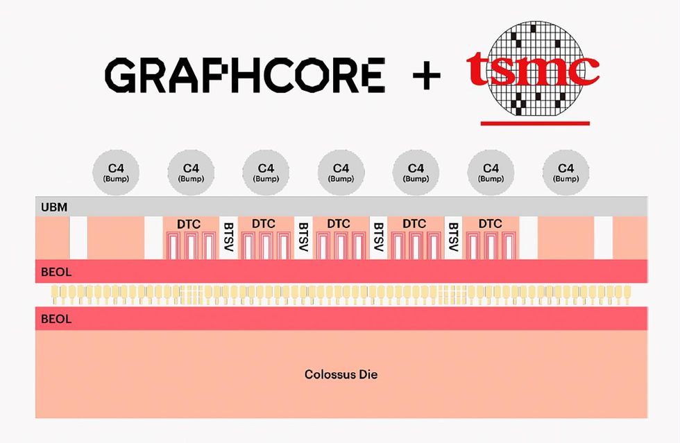 TSMC’s wafer-on-wafer stacking results in a processor chip [bottom] connected to a power-delivery chip [top] by copper pads [yellow]. Signals and power pass through the top chip from solder bumps [grey].Graphcore
Although the new product has no transistors on the power-delivery chip, those might be coming. Using the technology only for power delivery “is just the first step for us,” says Knowles. “It will go much further than that in the near future.”
Graphcore revealed some plans for that near future, announcing that it will build supercomputers that can train “brain-scale” AIs—those having hundreds of trillions of parameters in a neural network. The “Good” computer, named in honor of British mathematician I.J. “Jack” Good, would be capable of more than 10 exaflops—10 billion billion floating-point operations. Good would be made up of 512 systems with 8,192 IPUs along with mass storage, CPUs, and networking. It will have 4 petabytes of memory and a bandwidth of more than 10 PB per second. Graphcore estimates each supercomputer will cost about US $120 million and should be ready for delivery in 2024.
“When we started Graphcore...the idea has always been in the back of our mind to build an ultraintelligent computer that would surpass the capability of a human brain,” says Toon. “And that is what we are now working on.”
Competitor Cerebras Systems already planted its flag in the quest for brain-scale AI. It developed an external memory system and a way to connect multiple computers that would allow its computers to train neural networks with hundreds of trillions of parameters.


