
AMD lifted the hood on its next AI accelerator chip, the Instinct MI300, at the AMD Advancing AI event today, and it’s an unprecedented feat of 3D integration. MI300, a version of which will power the El Capitan supercomputer, is a layer cake of computing, memory, and communication that’s three slices of silicon high and that can sling as much as 17 terabytes of data vertically between those slices. The result is as much as a 3.4-fold boost in speed for certain machine-learning-critical calculations. The chip offers both contrasts and similarities to competing approaches such as Nvidia’s Grace Hopper superchip and Intel’s supercomputer accelerator Ponte Vecchio.
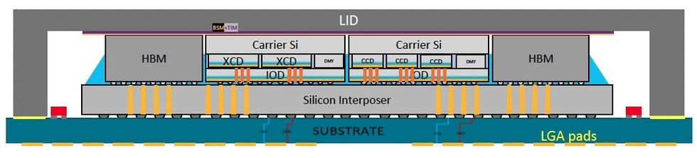
MI300a stacks three CPU chiplets (called compute complex dies, or CCDs, in AMD’s lingo) and six accelerator chiplets (XCDs) on top of four input-output dies (IODs), all on top of a piece of silicon that links them together to eight stacks of high-bandwidth DRAM that ring the superchip. (The MI300x substitutes the CCDs for two more XCDs, for an accelerator-only system.) With the scaling of transistors in the plane of the silicon slowing down, 3D stacking is seen as a key method to get more transistors into the same area and keep driving Moore’s Law forward.
 Compute and AI chiplets are stacked on top of I/O and cache chiplets in the MI300a.AMD
“It’s a truly amazing silicon stack up that delivers the highest density performance that industry knows how to produce at this time,” says Sam Naffziger, a senior vice president and corporate fellow at AMD. The integration is done using two Taiwan Semiconductor Manufacturing Co. technologies, SoIC (system on integrated chips) and CoWoS (chip on wafer on substrate). The latter stacks smaller chips on top of larger ones using hybrid bonding, which links copper pads on each chip directly without solder. It is used to produce AMD’s V-Cache, a cache-memory expanding chiplet that stacks on its highest-end CPU chiplets. The former, CoWos, stacks chiplets on a larger piece of silicon, called an interposer, which is built to contain high-density interconnects.
Similarities and differences between AMD and Nvidia
There are both similarities and differences to chief rival Nvidia’s approach. Just as Nvidia did in its Hopper architecture, AMD’s accelerator architecture, CDNA3, added the capability of computing with truncated 32-bit numbers called TF32 and with two different forms of 8-bit floating-point numbers. The latter attribute is used to speed the training of certain parts of transformer neural networks, such as large language models. They also both include a scheme that reduces the size of the neural network, called 4:2 sparsity.
Another similarity is the inclusion of both CPU and GPU in the same package. In many AI computer systems, GPUs and CPUs are separately packaged chips deployed in a 4 to 1 ratio. One advantage to joining them together in a single superchip is that both CPU and GPU have high-bandwidth access to the same cache and high-bandwidth DRAM (HBM) in a way that won’t trip each other up as they read and write data.
Nvidia’s Grace Hopper is such a superchip combination linking the Grace CPU to the Hopper GPU through Nvidia’s Nvidia NVLink Chip-2-Chip interconnects. AMD’s MI300a is as well, by integrating three CPU dies designed for its Genoa line and six XCD accelerators using its AMD Infinity Fabric interconnect technology.
But a casual glance at Grace Hopper and MI300 show some profound differences. Grace and Hopper are each individual dies that integrate all of a system-on-chip’s needed functional blocks—compute, I/O, and cache. They are linked horizontally, and they are large—nearly at the size limit of photolithography technology.
AMD took a different approach, one that it has followed for several generations of its CPUs and that rival Intel used for its 3D-stacked supercomputer accelerator Ponte Vecchio. The concept is called system-technology-co-optimization, or STCO. That means designers started by breaking the chip down into its functions and decided which functions needed which manufacturing technology.
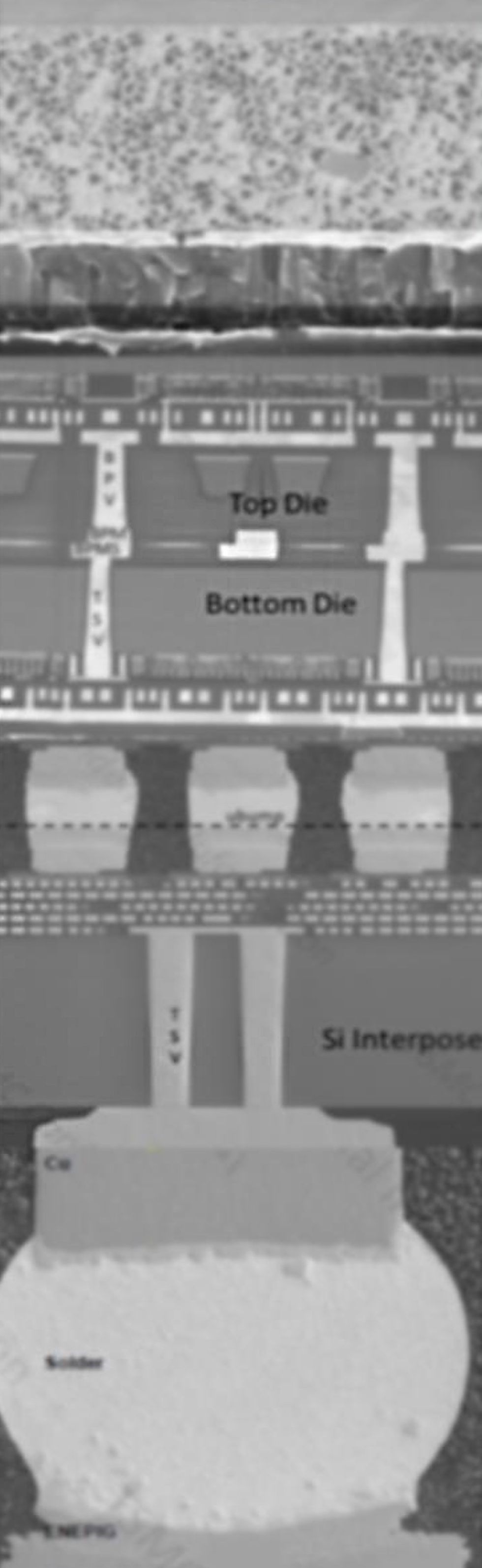 A slice of MI300 stack from the carrier silicon at the top to the solder ball at the bottom of the package.AMD
“What we wanted to do with MI300 was to scale beyond what was possible in a single monolithic GPU. So we deconstructed it into pieces and then built it back up,” says Alan Smith, a senior fellow and the chief architect for Instinct. Although it’s been doing so for several generations of CPUs, the MI300 is the first time the company has made GPU chiplets and bound them in a single system.
“Breaking the GPU into chiplets allowed us to put the compute in the most advanced process node while keeping the rest of the chip in technology that’s more appropriate for cache and I/O,” he says. In the case of the MI300, all the compute was built using TSMC’s N5 process, the most advanced available and the one used for Nvidia’s top-line GPUs. Neither the I/O functions nor the system’s cache memory benefit from N5, so AMD chose a less-expensive technology (N6) for those. Therefore, those two functions could then be built together on the same chiplet.
With the functions broken up, all the pieces of silicon involved in the MI300 are small. The largest, the I/O dies, are not even half the size of Hopper. And the CCDs are only about one-fifth the size of the I/O die. The small sizes make a big difference. Generally, smaller chips yield better. That is, a single wafer will provide a higher proportion of working small chips than it would large chips. “3D integration isn’t free,” says Naffziger. But the higher yield offsets the cost, he says.
Luck and experience
The design involved some clever reuse of existing technologies and designs, a few compromises, and a little luck, according to Naffziger, an IEEE Fellow. The reuse came in two instances. First, AMD was able to do the 3D integration with a degree of confidence because it had already been using the exact same pitch of vertical interconnects—9 micrometers—in its V-cache product.
As an optional add-on that AMD was able to charge extra for, V-cache offers little risk that poor yield or other problems will have a big impact on the company. “It’s been a great thing to enable us to wring out the manufacturing problems and all the design complexities of 3D stacking without endangering the main product line,” says Naffziger.
The other instance of reuse was a bit chancier. When the MI300 team decided that a CPU/GPU combination was needed, Naffziger “somewhat sheepishly” asked the head of the team designing the Zen4 CCD for the Genoa CPU if the CCD could be made to fit the MI300’s needs. That team was under pressure to meet an earlier deadline than expected, but a day later they responded. Naffziger was in luck; the Zen4 CCD had a small blank space in just the right spot to make the vertical connections to the MI300 I/O die and their associated circuitry without a disruption to the overall design.
Nevertheless, there was still some geometry that needed solving. To make all the internal communications work, the four I/O chiplets had to be facing each other on a particular edge. That meant making a mirror-image version of the chiplet. Because it was codesigned with the I/O chiplet, the XCD and its vertical connections were built to link up with both versions of the I/O. But there was no messing with the CCD, which they were lucky to have at all. So instead the I/O was designed with redundant connections, so that no matter which version of the chiplet it sat on, the CCD would connect.
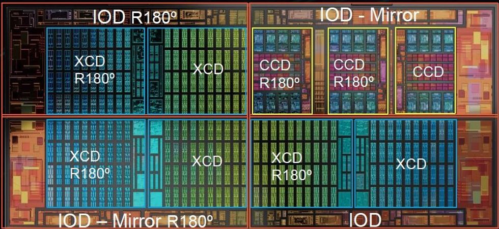 To get everything to line up, the IOD chiplets had to be made as mirrors of each other, and the accelerator (XCD) and compute (CCD) chiplets had to be rotated.AMD
The power grid, which has to deliver hundreds of amperes of current to the compute dies at the top of the stack, faced similar challenges because it too had to accommodate all the various chiplet orientations, Naffziger noted.


