Packaging has arguably never been a hotter subject. With Moore’s Law no longer providing the oomph it once did, one path to better computing is to connect chips more tightly together within the same package.
At Semicon West earlier this month, Intel showed off three new research efforts in packaging. One combines two of its existing technologies to more tightly integrate chiplets—smaller chips linked together in a package to form the kind of system that would, until recently, be made as a single large chip. Another adds better power delivery to dies at the top of a 3D stack of chips. And the final one is an improvement on Intel’s chiplet-to-chiplet interface called Advanced Interface Bus (AIB).
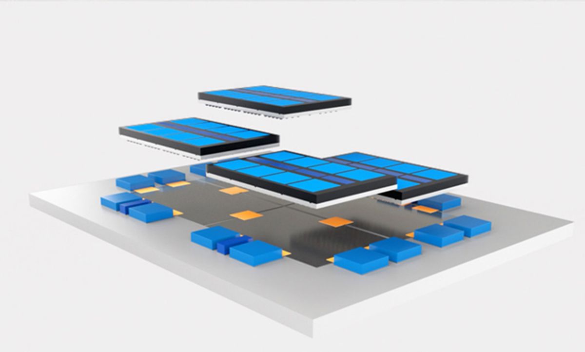
The first effort, dubbed Co-EMIB, is essentially a way of combining two existing Intel packaging technologies: EMIB (for embedded multidie interconnect bridge) and Foveros. The former bridges two chiplets over a short distance horizontally using a small piece of silicon embedded in a package’s organic substrate. The interconnect lines on silicon can be made narrower than on the organic substrate and can be packed together more tightly to form a high-bandwidth chip-to-chip connection. It’s used in systems like Intel’s Stratix 10 FPGA, which is actually an FPGA chiplet linked to two high-bandwidth DRAM and four high-speed transceiver chiplets in the same package.
Foveros is Intel’s 3D chip-stacking technology. It allows die-to-die connections that are just 50 micrometers apart, leading to high-bandwidth vertical connections. Through-silicon vias (or TSVs), conductors that pass vertically through the silicon of the bottom die, connect the stack to the package substrate.
Combining the two into Co-EMIB lets two or more Foveros stacks communicate through high-density EMIB bridges to build more complex systems. That might seem an obvious thing to do. But with connections only micrometers apart, an organic substrate that is hard to make perfectly planar, and a fairly large area to pattern, it was actually quite difficult.
“The scale of it becomes more and more critically [dependent] on how you can hold all your dimensional tolerancing through the assembly process,” says Johanna Swan, a fellow at Intel’s components research and technology development group. “The process tricks become more important in order to manage the size of structures. We’re able to show there’s a path for maintaining that dimensional stability over a larger area.”
The second research effort, Intel’s Omnidirectional Interconnect (ODI), essentially allows for EMIB-like vertical connections. These are larger than ordinary through-silicon vias—about 70 micrometers across versus a typical TSV’s 10 micrometers. The large diameter makes them especially well suited to deliver power to the top die in a 3D stack, according to Swan. “As you scale that area, you get cleaner, more efficient power delivery,” she says.
MDIO, the product of the third effort, should be available in 2020 according to Intel’s Semicon West presentation. It offers 200 gigabytes per second per millimeter of chip edge versus AIB’s 63 GB/s-mm, and it uses 0.50 picojoules per bit versus AIB’s 0.85. Intel compared MDIO to TSMC’s LIPINCON technology, which is also expected in 2020 and delivers 67 GB/s-mm at about the same picojoules per bit.
Intel R&D will continue to try to increase the number of bumps—the solder ball on/off ramps from a chip—available in a given area, says Swan. But ultimately, getting rid of solder is the goal. The intermetallic interface between the solder and the copper interconnects limits current, so Intel, and others, are exploring a technology called hybrid bonding, which uses a dielectric material and heat to connect one chip’s copper pads to another without solder.
Samuel K. Moore is the senior editor at IEEE Spectrum in charge of semiconductors coverage. An IEEE member, he has a bachelor's degree in biomedical engineering from Brown University and a master's degree in journalism from New York University.


