Semiconductors

The Art of Failure 2012

Failure analysts show off the strange stuff they find in their microscopes

Photo: Lim Saw Sing/Infineon Technologies
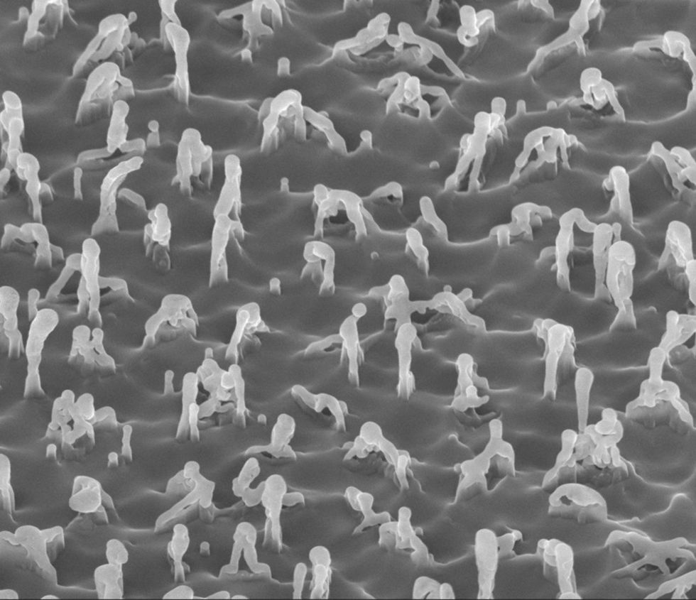
People on the Beach: That’s what Lim Saw Sing saw in this scanning electron microscope image. Lim, who works at Infineon Technologies’ facility in Kulim, Malaysia, exposed a polyimide surface to etching by reactive ions. The resulting image won first prize at the 2012 IEEE International Symposium on the Physical and Failure Analysis of Integrated Circuits (IPFA 2012).
Photo: Foo Fang Jie/AMD
Wings: Advanced Micro Devices analyst Foo Fang Jie found this set of angelic wings while examining a fracture in a sample of silicon. It won second prize.
Photo: Tan Lee Koon/Systems-on-Silicon Manufacturing Co.
The Hope Terrace: The chipping at the edge of a silicon wafer, when examined under a scanning electron microscope, looks like an inspiring bit of geography, according to third-prize winner Tan Lee Koon.
Photo: Lim Chan Way/Infineon Technologies
Mysterious Jungle: A membrane structure [top] adheres to a bit of carbon tape to form a strange forest in this microscopy image.
Photo: Lee Chee Hiong/Systems-on-Silicon Manufacturing Co.
The Happy Frog: Systems-on-Silicon analysts were inspired by the way this “frog” seemed to look forward to the next challenge.
Photo: Amy Ng/Angelina Lau/Micron Technology
Silver Leaves: These cabbage-like growths are silver sulfide crystals on a resistor network. The crystals increased the resistance to the point where the network stopped conducting.
Photo: Jacqueline Kwa/AMD
The Royal Elephant: Advanced Micro Devices analysts thought this transmission electron microscope image of a silicon sample looked like an elephant in a headdress preparing to usher in the king.
Photo: Wu Xing/Pey Kin Leong/Singapore University of Design and Technology
Big Nose: A resistive RAM device made of nickel [top], halfnium dioxide [middle], and silicon [bottom] melted down during testing, resulting in an adorable clown face.
Photo: Khoo Bing Sheng/WinTech Nano-Technology
Fist of Victory: Perhaps foreshadowing the 2012 Olympics, engineers at WinTech Nano-Technology created this 20-micrometer-wide sculpture from copper using focused-ion-beam nanofabrication.
Photo: Joel B. Hosmillo/Analog Devices
Lunar Eclipse: The moon is really a capacitor, part of a low-pass filter circuit damaged by an electrostatic discharge.
IEEE Spectrum
FOR THE TECHNOLOGY INSIDER

Follow IEEE Spectrum

Support IEEE Spectrum

IEEE Spectrum is the flagship publication of the IEEE — the world’s largest professional organization devoted to engineering and applied sciences. Our articles, podcasts, and infographics inform our readers about developments in technology, engineering, and science.