
Even after you don a bunny suit and get deep inside Fab 8, it’s hard to get a sense of scale. Rows upon rows of tall machines, known as tools, dominate this US $12 billion GlobalFoundries facility, built amid forest north of Albany, N.Y. Carriers containing silicon wafers zip overhead along ceiling-mounted tracks, like tiny inverted roller coasters. If your timing is good, you’ll be standing by a tool when one of those carriers descends to join it, moving a wafer along to the next step in the three-month-long process it takes to turn a dinner-plate-size disk of raw silicon into chips that could be used inside smartphones, personal computers, and servers. That’s right: Begin making a microprocessor here on New Year’s Day and it may just be finished by the start of spring.
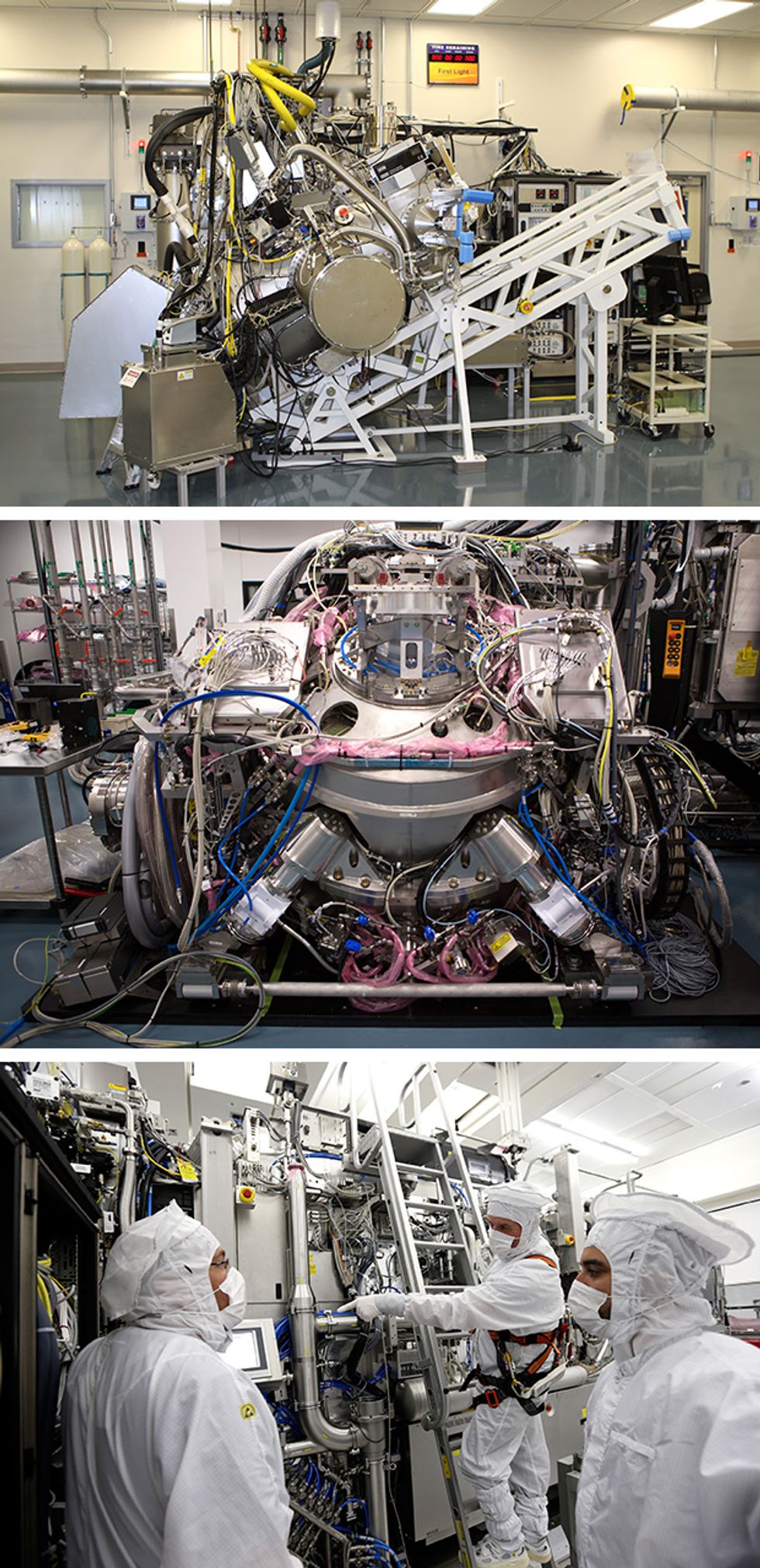 Inside the Machine: To generate EUV, pulses of CO2 laser light are sent into a vessel (top and middle) where they collide with tiny tin droplets to create plasma. This partially assembled EUV scanner (bottom) at ASML’s headquarters in Veldhoven, Netherlands, is one of the company’s more recent models.Photos: ASML
More than 60 times in the course of this advanced manufacturing process, a wafer will be coated with a light-sensitive substance and enter a light-tight box called a scanner. There, in a process called photolithography, laser light shines through a patterned surface and casts shrunken versions of that pattern onto the wafer, creating the ultrafine features that are needed to build the minute transistors and wiring inside cutting-edge processors.
There is little to distinguish these lithography machines from the myriad other tools in this vast ocean of automation. There is no big red sign that flashes “Critically important step here!” But lithography, explains Fab 8 general manager Tom Caulfield, “is the heartbeat of the fab.”
Think of these scanners as the front line of Moore’s Law, the repeated doubling of the density of integrated circuit components that has defined more than 50 years of astounding technological progress. For decades, a steady series of remarkable breakthroughs, many of them in photolithography, have enabled chipmakers to repeatedly shrink chip features, keep the length of R&D cycles under control, and economically pack more and more transistors on a chip. Those advances have taken us from chips with thousands of transistors in the early 1970s to billions today.
But to keep the good times rolling, GlobalFoundries and other leading-edge chipmakers won’t be able to rely on the brilliant lithographic advances of the past. And so they’re contemplating another radical shift, one that could prove to be the most challenging yet.
For the entirety of its existence, semiconductor lithography has been done with electromagnetic radiation that was more or less recognizable as light. But for the change chipmakers are now weighing, the radiation is something else altogether. It’s called extreme ultraviolet (EUV) radiation, but don’t let that name fool you. Unlike the ultraviolet light used in today’s scanners, EUV can’t travel in air, and it can’t be focused by lenses or conventional mirrors.
And it’s also difficult to produce; the process begins by firing laser light at a rapid-fire stream of tiny molten tin droplets. The hope is that scanners built to use the resulting 13.5-nanometer light—a wavelength that is less than a tenth of what is used in today’s most state-of-the-art machines—will save chipmakers money by allowing them to print in a single step layers that would otherwise require multiple exposures.
But creating EUV systems that are bright and reliable enough to operate in the fab—nearly 24 hours a day, 365 days a year—has proved to be a monumental engineering challenge. For many years, EUV faced significant skepticism and repeatedly failed to live up to predictions that it was almost ready for prime time.
Now, though, the technology really does seem to be turning a corner. The brightness of the EUV light source made by Dutch lithography-tool manufacturer ASML Holding seems to be closing in on a figure long targeted for commercial production. ASML, which has emerged as the technology’s standard-bearer, is now shipping EUV scanners that it says should be ready to mass manufacture leading-edge microprocessors and memory starting in 2018. The world’s most advanced chipmakers are working hard to determine when and how these machines will be incorporated into their production lines.
The stakes are high. Moore’s Law is facing significant challenges, and no one is sure how the semiconductor industry—which grossed more than $330 billion last year—will navigate the next five or 10 years or what a post-Moore’s-Law semiconductor industry will look like. A decline in revenues might be inevitable. But if keeping the “law” in effect avoids, say, a 15 percent drop in the industry’s income, that would keep an amount of money flowing that is twice as great as the total revenues of the U.S. video game industry.
The fineness of the details that can be made with a photolithographic system depends on several factors. But a powerful way to make dramatic improvements is to shorten the wavelength of the light it uses. For decades, lithographers have done just that, shifting their wafer-exposing tools from operation at the blue edge of what’s visible to the human eye down to successively shorter wavelengths in the ultraviolet part of the spectrum.
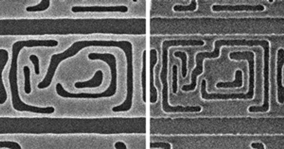 Curves and Corners: EUV promises to create sharper shapes (right) than those that can be created through multiple patterning with today’s 193-nanometer light (left). The lines in these micrographs have a minimum width of 24 nm.Images: ASML
In the late 1980s, the semiconductor industry was beginning the process [PDF] of shifting from mercury lamps to lasers as the light source of choice, reducing the wavelength from 365 nm to 248 nm in the process. But some researchers were already contemplating a far bigger jump, into the X-ray range. Hiroo Kinoshita, then at the Japanese telecommunications firm NTT, reported the results of early work on this idea way back in 1986, using 11-nm radiation. Others, at AT&T Bell Laboratories and at Lawrence Livermore National Laboratory, also explored the technology independently. In 1989, some of these researchers met and traded notes at a lithography conference. In ensuing years, research into the notion got infusions of investment from government and industry.
ASML and several partners began work on what was by then known as EUV lithography in the late 1990s. That was when Anton van Dijsseldonk, who grew up in Veldhoven, the Dutch town where ASML is headquartered, became the company’s first full-time employee on the project. “The end of Moore’s Law was predicted,” he recalls, and the semiconductor industry was hunting for ways to keep resolution improvements going. Chipmakers were also struggling to improve overlay—the ability to put a wafer back in the scanner again after its peregrinations through the fab and have the next set of patterns print in exactly the right place. “People were looking in those days at the alternatives,” van Dijsseldonk says, “and EUV was the exotic one.”
But from the beginning, ASML’s EUV researchers were convinced they could make the technology work—and that it would be the most economical option for chipmakers. Before the decade was out, the company had decided to build demonstration scanners that could be used by other researchers to test the approach.
Nothing about it was easy. Physics offers few favors for engineers hoping to cast patterns with what are essentially X-rays. At 13.5 nm, the wavelength the company ultimately chose, light is readily absorbed by many materials. Even the air we breathe “is absolutely black,” absorbing every last bit of the radiation, van Dijsseldonk notes. So he and his colleagues realized early on that the only way an EUV scanner could work was in vacuum, with each wafer entering and leaving the scanner through an air lock.
And then there’s the problem of bending the radiation. EUV is also absorbed by glass, so directing it through the machine would require a shift from lenses to mirrors. And not just any mirrors. A simple polished surface would not be nearly reflective enough, so they’d have to use Bragg reflectors—multilayer mirrors that can constructively reinforce many small reflections into a single, reasonably strong one.

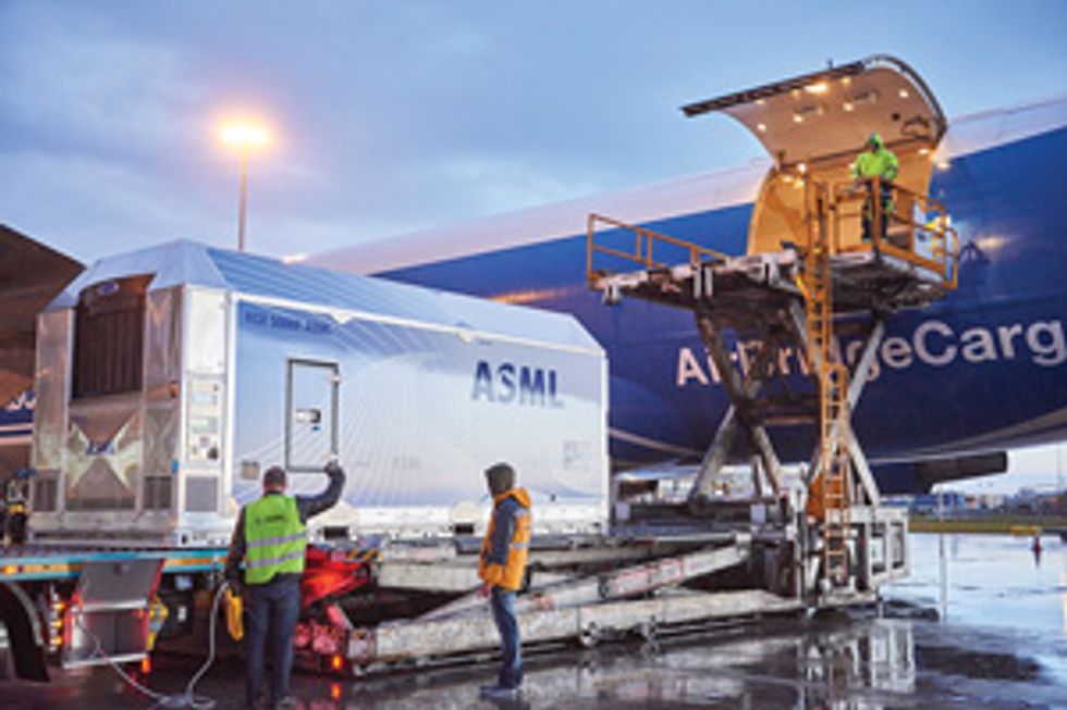
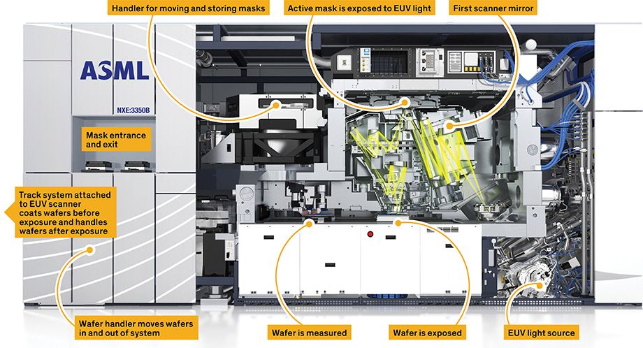
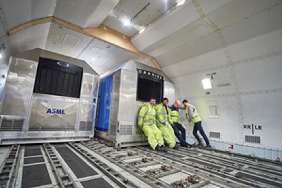 Headed East: A portion of an ASML NXE:3350B EUV scanner is loaded onto a 747-400 extended-range freighter at the Amsterdam Airport Schiphol in the Netherlands, for shipment to a customer. The scanner is split into nine parts (some larger than others) for shipping.Photos: ASML
Today, the mirrors inside ASML’s EUV machines consist of 40 pairs of alternating silicon and molybdenum layers—each just a few nanometers thick. Zeiss, the company that developed these mirrors, constructs their aspheric surfaces with great precision. But at the end of the day, van Dijsseldonk says, “if you do it fantastically [well], you get a mirror with a reflectivity of 70 percent.” That level of reflectivity means that, for every pair of mirrors used in the system, the light is cut by half. And a scanner could easily require a dozen mirrors to take light from the source to the mask—itself a mirror—and then on to the wafer. After an EUV beam has traversed this gauntlet, less than 2 percent of the light may be left.
The less light that reaches a wafer, the longer a wafer must remain in the scanner to be exposed. And in a fab, time means money. For EUV to make it into commercial use, it needs to be able to compete with the cost of existing lithographic methods. So the losses among the mirrors have to be compensated by a radiation source that is extremely bright. And that proved to be really, really hard to engineer.
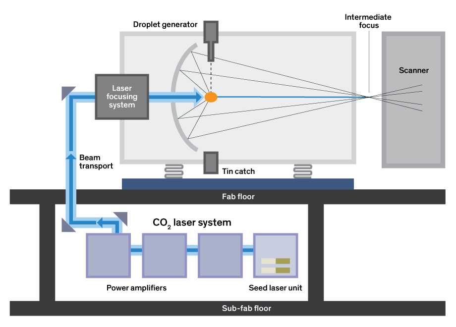
In the early days, EUV researchers used just about everything they could think of to generate X-rays, including lasers and particle accelerators. But the method that won out, which seemed to offer a practical and economical way to get sufficient brightness, employs plasma. Zap the right material with a powerful enough laser or electric current and you can separate electrons from the atoms they’re attached to. The resulting plasma will radiate EUV as the superhot blob cools back to its prezapped state.
The oft-repeated target for such plasma-based light sources has been 250 watts at the intermediate focus, the location where the EUV light exits the source and enters the scanner. That level of light would enable the machine to produce in the neighborhood of 125 wafers per hour, a mass production target that is about half the rate of today’s advanced 193-nm machines.
But for a number of years, progress was slow, and brightness improvements consistently lagged behind predictions. By 2011, some five years after ASML delivered its first test scanners to two customers, one of the leading light-source developers, San Diego–based Cymer, had succeeded in developing a source that could consistently deliver 11 W. “We probably underestimated how difficult it would be,” concedes ASML’s Hans Meiling, who is responsible for EUV product marketing. In the end, in an effort to accelerate development, ASML put in a bid for Cymer, formally completing the reported €3.1 billion acquisition in 2013.
To create EUV light, Cymer uses an approach called laser-produced plasma, which fires 50,000 microscopic droplets a second of ultrapure molten tin across a vacuum chamber, hitting each with powerful CO2-laser light generated by a series of amplifiers derived from a design originally used for metal cutting. When a laser pulse hits a molten tin droplet, it heats it up into an EUV-emitting plasma. A collector mirror reflects light created in this process and casts it into the scanner. Because the approach generates EUV light as well as tin debris, hydrogen gas constantly flows across the collector mirror to keep it from being rapidly covered with a layer of tin.
“The first time I heard about it, I thought it was insane,” admits ASML’s Alberto Pirati, who joined the company’s EUV light-source program in early 2013. But little by little, the team achieved the seemingly impossible. One of the biggest breakthroughs came with the introduction of a technique the Cymer team began exploring before being acquired by ASML. They found that if they fired a “prepulse” before the main laser, they could flatten each tin droplet into a pancake, creating more surface area for the main laser to hit and increasing how much of the tin droplet was converted to plasma. The change has boosted the laser-to-EUV conversion efficiency from a meager 1 percent to some 5 percent. Earlier this year, thanks to the prepulse and other optimizations, ASML reported that it had reached 200 W in the lab. Another light-source developer, Gigaphoton, has also reported great progress. The long-awaited production target of 250 W no longer seems far off. But the true test of whether EUV is ready to go into production will happen in the labs and fabs—and spreadsheets—of ASML’s chipmaking customers.
Nobody doubts that EUV machines can make fine features. Go to a semiconductor conference and you’ll probably come across a presentation with sharp-looking micrographs of EUV-made patterns, juxtaposed against blurrier ones made using today’s conventional methods.
The question now is what role EUV will play in the mass production of major commercial chips—and when it will do it. Certainly, the cost of adopting EUV seems daunting. The list price of ASML’s newest EUV machine exceeds €100 million, more than twice that of an average 193-nm scanner, says spokesperson Niclas Mika. It is about the height and width of a New York City bus and is shipped in multiple 747s. Customer estimates suggest such a machine, run at mass-production levels, could consume some 1.5 megawatts or so of electricity, significantly more than a 193-nm machine.
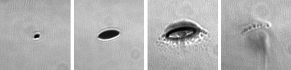 The Evolution of a Droplet: To create EUV light, molten tin droplets are flattened by one laser pulse and then converted to light-emitting plasma by a second pulse.Images: ASML
But a simple comparison of specs won’t capture all the costs of manufacturing. Today’s state-of-the-art 193-nm lithographic systems can produce chip features with dimensions that are a small fraction of that wavelength. This feat was made possible by two major breakthroughs. The first was immersion lithography, which places water between a silicon wafer and the optics that project a pattern onto it. The second was multiple patterning, which splits the process of making the features in a layer into two or more steps. To create a set of closely spaced holes, for example, a wafer can be run once through the scanner to fashion half of them, and then again to fashion the other half, slightly offset. Because wafer position can be determined with great precision, multiple patterning lets engineers create features that are more closely spaced than would be possible in one step. In principle, the more steps used, the finer the features. But each addition makes the process of bringing a chip into the world costlier and more complex.
Today, GlobalFoundries uses triple patterning when it makes its 14-nm chips, the most advanced ones currently created in Fab 8. This means that, for certain critical layers, a chip takes two extra passes through a scanner—and every other tool that is used to make those layers. And the company anticipates going to quadruple patterning at 7 nm, its next chip generation, says George Gomba, who is leading the company’s task of evaluating the technology at a SUNY Polytechnic Institute facility in Albany, along with colleagues from IBM.
For now, GlobalFoundries plans to roll out its 7-nm chips in 2018 without EUV, but it is reserving the option of pulling the technology in when it is ready. A key question for Gomba and his colleagues is when the cost of EUV will break even with multiple patterning. And it’s a very tricky question to answer because it depends on a number of unknown factors, including how bright EUV light sources will become and the uptime of an entire EUV lithographic system—the percentage of time it’s actually available to be used.
GlobalFoundries and IBM are not the only ones that have poured money into EUV. In 2012, Intel, Samsung, and Taiwan Semiconductor Manufacturing Co. (TSMC) committed a total of €1.38 billion in R&D funding to ASML for next-generation lithography research (the same deal garnered ASML €3.85 billion for nonvoting shares in the company). ASML’s Meiling estimates about 4,000 people work on EUV for the company, a figure that does not include the researchers at leading chipmakers and research institutions with EUV programs of their own.
The reason for all this investment is not only that EUV is hard but that chipmakers are coming around to the idea that, soon, they may not be able to move forward without it. If you ask Anthony Yen, who leads EUV lithography development at TSMC, how critical EUV is to Moore’s Law, he won’t beat around the bush: “Totally critical. 100 percent critical. Very, very critical.” TSMC expects to adopt EUV in 2020, when the company aims to begin producing chips on its 5-nm manufacturing line.
For now, though, there are still some engineering challenges. At the top of Yen’s list is protecting the mask, the stencil-like surface that carries a pattern to be printed on the wafer. Just as the optical components of the EUV scanner are reflective, so too is the mask. And here, once again, the pesky matter of reflectance becomes an issue.
In a 193-nm immersion machine, the mask is protected by a thin film called a pellicle, which is suspended a short distance away and stretched across it like a piece of plastic wrap. At current feature sizes, a piece of dust too small to see with the naked eye is still big enough to blot out hundreds of transistors. Thanks to the magic of optics, if a piece of dust falls on the pellicle, it will be too out of focus to create a pattern on the wafer.
But these 193-nm pellicles aren’t designed to be transparent to 13.5-nm light; EUV would quickly obliterate them. ASML planned to build the scanners without pellicles, but chipmakers weren’t comfortable with the potential downside. “If one particle gets on a mask,” Yen explains, “every single die on your wafer is damaged. Basically, you can end up with zero yield.” Months of work and, depending on the number of wafers produced, tens or even hundreds of thousands of dollars’ worth of chips would be lost.
As a result, ASML has been researching ways to make a pellicle that can withstand the harsh onslaught of EUV radiation. The pellicle has to be as transparent as possible, so that little additional light is lost before it gets to the wafer. And it’s doubly difficult in this case: Because EUV masks are reflective rather than transmissive, light must go through a pellicle twice—once on the way in and once on the way out.
There are still other challenges with EUV that its potential customers want to see resolved before they commit to the technology. One is the ability to make EUV masks free of defects—and develop efficient ways to confirm that they are in fact defect free. Another piece of the puzzle is the photoresist—the light-sensitive layer that is coated on a wafer to take a mask’s pattern.
Today’s resists, known as chemically amplified resists, are made from polymeric chains of molecules that multiply the effect of incoming photons. But these materials are not especially efficient absorbers of EUV light, explains Andrew Grenville, CEO of the EUV-resist startup Inpria. What’s more, the recorded image tends to blur slightly as the light-triggered amplification reaction diffuses through the material. To make finer features than we have today, “you really need much smaller and more robust building blocks,” Grenville says. Inpria is working on a resist made of smaller tin-oxide components that are designed to absorb EUV five times as readily and create patterns without amplification.
Will it all be ready in time to keep Moore’s Law from dissolving, either permanently or temporarily? Lithography expert Chris Mack doubts that all the pieces will come together for chipmakers by 2018. Planning for a new chip-manufacturing generation happens years in advance. Making a commitment to use EUV in just a few years’ time, he says, “is too risky.”
Mack, a notorious EUV skeptic who once wagered his Lotus Elise sports car against the technology, does, however, admit to a “glimmer of hope” for it. Chipmakers are struggling to keep miniaturization on track and costs under control; the timing between successive chip generations seems to be getting longer, and chip features are not shrinking as aggressively as they used to. These struggles could give EUV an opening, he says: “There’s a real possibility that this slowdown in Moore’s Law could enable EUV to have enough time to catch up.”
Enough time, that is, before costs cause Moore’s Law to grind to a halt. EUV may well reach a point where it is ready for adoption and will reduce manufacturing costs, Mack says. But by that point, he says, the overall cost of the next generation of advanced chips may prove too much—and the performance benefits not impressive enough—for chipmakers to pursue it. Already, Mack says, older chip-manufacturing generations are staying in the mix longer: “I think we’re going to see the marketplace splitting up and lots of companies doing lots of different things.”
As it has in the past, the fate of Moore’s Law will hinge not only on how finely we can print features but on how well physicists and engineers can keep improving the resulting transistors and circuits. Even a rapid-fire sequence of tin plasma flashes won’t be able to shed any light on exactly when the world’s greatest technological winning streak will finally end. But it just might light the path ahead.
A version of this article appears in the November 2016 print issue as “The Molten Tin Solution.”