
What a difference a year makes. Only 12 months ago, the future of lithography, the core technology of the multibillion-dollar-a-year business of making chips, seemed straightforward. Optical lithography, the technique of using light to print onto a silicon wafer the wires, transistor parts, and everything else that make up an integrated circuit, was about to go the way of the Model T. Pressed to the very limits of its ability to print the vanishingly narrow arrays of lines, spaces, and contacts needed for upcoming generations of ICs, it would soon be replaced by extreme ultraviolet lithography, a sleek new technology propelled by the considerable commercial momentum of Intel Corp., Santa Clara, Calif.
But now, out of nowhere, a new technique has emerged that promises to breathe new life into optical lithography and put off until the next decade its replacement by extreme ultraviolet. And it seems to be just in time. In the semiconductor industry, where a good year’s sales add up to a quarter-trillion dollars, a three-year reprieve that lets researchers work out the kinks in the still-experimental technology of extreme ultraviolet lithography might just turn out to be the most timely and valuable pause in business history.
The upstart technology is known as immersion lithography. It accomplishes its life-extending wizardry by adding a tiny film of water between the optical system’s projection lens and the silicon wafer, allowing lithographic systems to print wires and spaces once thought impossibly narrow.
Even in an industry accustomed to accomplishing the seemingly impossible every 20 months or so, experts are nevertheless amazed by the speed with which the new optical technology has burst onto the scene. As a general rule, new lithographic systems take decades to develop. But in a space of less than two years, immersion has moved from an unknown to being the technology most likely to be used from 2007 through at least 2010.
The Three Major Lithography-System companies—ASML (the largest), in Veldhoven, the Netherlands, and Canon Inc. and Nikon Corp., both in Tokyo—consider its promise so great that they have started crash programs to develop the technology and now plan to deliver immersion systems to their chip-making customers within the next year or two. This is an incredible schedule, even in the fast-paced semiconductor industry, according to Walt Trybula, senior fellow, International Sematech, the Austin, Texas–based consortium of makers of semiconductors and of the tools used in their manufacture. “In a little more than a year, we’ve gone from a concept of plausibility to a schedule for delivery of tools. This has not happened before in the industry for a major technology revision,” says Trybula, who is also a fellow of the IEEE. By the end of last year, Nikon’s in-house development system had already printed components with dimensions smaller than 65 nanometers—a key requirement for the next generation of chips. Both ASML and Nikon have said that they will soon begin shipping systems to semiconductor development labs for further testing and evaluation in a setting more like that of a commercial plant. And Nikon has announced plans to start mass-producing them in 2006.
Yet another sign of the technology’s ascendance came at the recent Lithography Forum organized by Sematech. The purpose of the meeting, held this past January in Los Angeles, was simply to sort out the dazzling profusion of lithographic technologies developed to prepare for the anticipated crisis in optical lithography. But the meeting came close to being a coronation for immersion lithography.
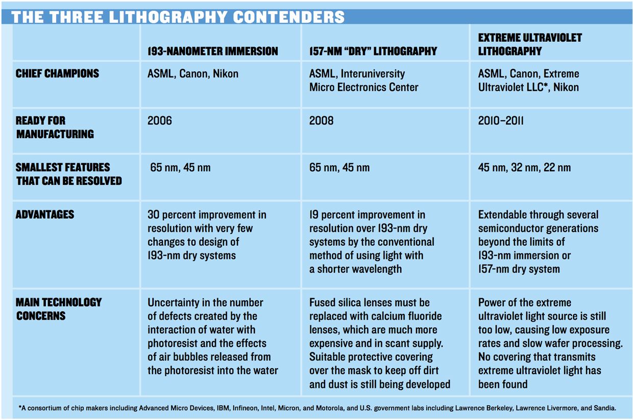
At the forum, developers of each technology, including the extreme ultraviolet approach heavily backed by Intel, gave a status report. At the end of the conference, surveys polled the opinions of the attendees about the strengths and weaknesses of each approach. They were asked to rate the production readiness of each system and to predict the year that the technology would be ready for manufacturing. They were also asked detailed questions about each aspect of the technology and its infrastructure, the ability to produce wires at the required dimensions, and the cost. And they were asked which technology was most likely to be used to manufacture wafers in 2007, when the narrowest lines on ICs are expected to be 65 nm, and in 2009, when they will dip down to a breathtaking 45 nm.
The overwhelming winner: immersion lithography. Attendees spurned extreme ultraviolet even though most of them thought that it would be ready for manufacturing in just five years.
To understand the ingeniousness of immersion lithography, start with its plain-old “dry” counterpart. On a wafer of prepared silicon, the current method produces hundreds of ICs, each consisting of perhaps hundreds of millions of transistors along with the interconnecting wires that make up a single IC. On each wafer, the process of creation takes place IC by IC and layer by layer, starting with the transistor electrodes and ending with the contacts between different wire layers.
At the heart of this process, a beam of light passes through a stencil-like chrome-covered transparent plate called a mask. The chrome has been patterned with a magnified image of the particular layer of the IC being created in that step—for example, the transistor contacts. Where the chrome has been removed, the light passes through the mask and is focused by the projection lens onto the wafer, which has been coated with a photosensitive material. After one IC site has been exposed to the patterned light, the movable stage that supports the wafer repositions it under the projection lens so that a different IC site can be exposed.
After all the IC sites on the resist-covered wafer are exposed to the light, the wafer is taken from the lithography system, and the now-soluble resist is rinsed away, leaving a negative image in photoresist of the IC layer that is to be created. After the rinsing step, the wafer undergoes various other processes, such as ion implantation or deposition, which depend on the particular layer being formed. The remaining resist is then removed and a fresh layer applied before the wafer is put back in the lithography system for the next layer.
This process has worked amazingly well for about four decades, but it is now entering a twilight phase. The root cause of its anticipated demise is the wavelength of the light that the system uses to print all those layers of patterns. The resolution of the system—the narrowness of the wires and the spaces between them that the system is capable of printing—depends directly on the wavelength and inversely on a property of the optical system called the numerical aperture. So, to print really small details, you want either a small wavelength, or a large aperture, or, ideally, both.
The numerical aperture, roughly analogous to the f-stop in photography, is related to the product of two key characteristics of the lithography system: one is the widest angle through which light passing through the lens can be focused on the wafer; the other is the refractive index of the medium through which the light passes on its way to the wafer. The refractive index, in turn, is the ratio of the speed of light in a vacuum over its speed in the medium.
Air has a refractive index of 1, and a lithographic system operating in air has a numerical aperture between 0 and 1. Recall that what you want is the largest possible numerical aperture. One way of getting it, clearly, is by operating your lithographic system in a medium with a refractive index greater than that of air—in other words, greater than 1. But more on that later. Wouldn’t it just be simpler to reduce the wavelength of the light? Yes, up to a point. And we’re getting very close to that point.
To resolve the ever-shrinking wire widths demanded by an industry intent on shrinking them by 30percent every two years or so, engineers and researchers have been pursuing the twin strategies of reducing wavelengths while also making lenses bigger to increase the numerical aperture. Almost all the while, they’ve been fretting that they are getting to the end of the line as far as optical wavelengths are concerned.
But each time the resolution of optical lithography seemed about to reach its limit, Herculean technical advances kept the cycles going. From wavelengths of 450 nm and numerical apertures of 0.2 in early lithography systems, the wavelength now stands at 193 nm with numerical apertures of 0.85 in today’s state-of-the-art commercial lithography systems. These will produce ICs with more than half a billion transistors and wires and spaces less than 100 nm wide.
Now, however, the approach of reducing wavelengths has come up against a brick wall. The reason is simple: light with a wavelength smaller than 193 nm is absorbed, rather than passed, by the fused silica (amorphous silicon dioxide) lenses that focus and project the light onto the wafer.
For optics, though, engineers have one more Herculean technical trick up their sleeves: immersion lithography. Though the strategy of reducing the optical wavelength has gone as far as it can go, the technique of increasing the aperture has not. For the next few years, big gains will come not only from making bigger lenses, but also from changing the refractive index of the medium. These lithographic systems will continue to use 193-nm light, but they will put water, not air, between the lens and the wafer. Water has a refractive index of 1.4, so the numerical aperture of the system grows by a factor of 1.4 in comparison with that of its dry counterpart, with a corresponding improvement in resolution.
It gets even better. By using water, you can exploit a fortuitous quirk of physics, having to do with the way light bends when it passes through the interface between two materials at any angle other than perpendicular. The amount of bending is equal to the ratio of the refractive indices of the two materials; it’s why a stick that is perfectly straight appears bent when part of it is poking out of the water. Because the refractive index of water is very close to that of the fused silica that makes up the projection lens, the light bends less when it passes from the lens to the water than it does in a dry system, where the light passes from the lens into air. This allows immersion-lithography developers to increase the numerical aperture still further by building bigger lenses that collect more light.
Perhaps most comforting of all to the lithography community is simply the similarity of 193-nm immersion to its dry counterpart, which is already being used in commercial fabrication facilities. Technicians will be able to use many of the same optical and mechanical elements, including lenses and wafer stages, and much of the infrastructure, including masks and photoresists.
Another important consideration is the number of wafers that the system can process in an hour, absolutely vital to chip makers, whose profits depend on how fast they can churn out ICs. Current 193-nm equipment processes more than 100 wafers of a single circuit level in an hour, and immersion systems should be just about as fast. Other approaches have yet to demonstrate throughputs anywhere near as high.
Though it sounds straightforward, the big change in 193-nm immersion lithography—putting water between the projection lens and the wafer—is the major challenge. Developers have tried a number of ideas, including dunking everything—the projection lens, the wafer, and the movable stage that supports and positions the wafer—into a pool of water. The problem with this approach is that moving the stage through water is much more difficult than moving it through air, as you can well imagine if you’ve ever tried to run in a swimming pool. This reduces throughput, because it is extremely difficult to rapidly reposition the wafer to the next IC location.
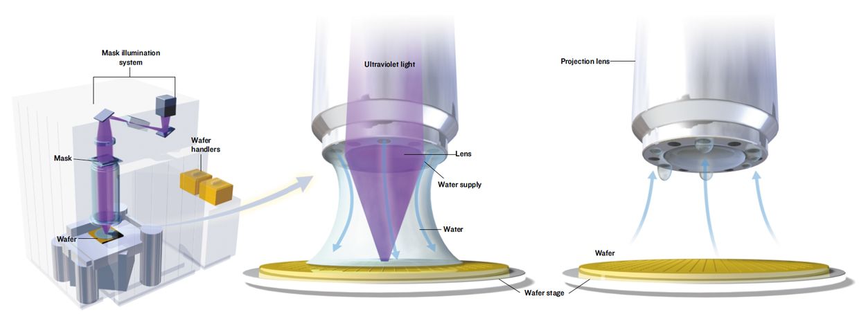
Researchers are therefore now concentrating on a different tack: injecting a small film of water between the wafer and the lens. This film covers just the IC site being exposed, rather than the entire wafer. Each company has its own technique, but a typical approach is to squirt a bit of water through an opening in the lens housing, expose the site, then suction up the water with a vacuum before the wafer is moved to the next IC location, where the process is repeated [see illustration, "Getting Wafers Wet"].
Although system developers are confident they will find clear sailing all the way to volume production, some observers are not so sure. Those with reservations include Kurt Ronse, lithography department director of the Interuniversity Micro Electronics Center (IMEC), an independent research organization in Leuven, Belgium. His main concern is that water in contact with the photoresist will introduce defects. "There could be a number of new defect mechanisms that pop up," he says, "which will require some time to be resolved. I don’t think it will be a showstopper, but it may delay the insertion of immersion lithography for a couple of months to a year."
"Up until this point," adds Giang Dao, Sematech’s director of lithography, "you had resist interacting only with air. Now you have resist coming into contact with water running very fast on and off the wafer."
Because water is an optical element in immersion systems, its properties affect the ability of the system to print defect-free lines and spaces. Several properties of water can affect defect levels: particle impurities, temperature variations, and thickness uniformity of the water layer. Researchers now believe that these properties are well enough under control so as not to be a source of defects.
But developers are still fretting about the occurrence of bubbles in the water layer, which can scatter the light from the lens, causing blurring and distortion of the projected image. Two sources of bubbles are air dissolved in the water and air introduced into the water as it is ejected from the nozzles. Researchers now believe that removing the gas from the water before it is sprayed onto the wafer—a process called degasification—can eliminate the first cause, and careful design of the nozzles can remove the second. However, air trapped on the surface of the photoresist can also create bubbles as the water flows over the surface of the wafer.
Of course, researchers are not ignoring the issue of water-induced defects. "But," says Dao, "systems will have to be running in a manufacturing environment before quantitative measurements of defect levels can be obtained."
Significant though these issues may be, they nevertheless don’t inspire quite the same anxiety as those plaguing some of the alternatives. Consider extreme ultraviolet. Despite its name, it actually uses soft X-rays with a wavelength of 13.4 nm. Instead of lenses and conventional masks, it relies on mirrors made from many alternating layers of atomically smooth silicon and molybdenum. Foremost among the challenges here is the power of the source of soft X-rays. One current approach is to bombard a target—which could be made of xenon, tin, lithium, or a number of other materials—with a powerful laser, to produce a plasma that radiates energy when the elements of the plasma recombine. Another technique is to magnetically compress xenon or tin to very high temperatures.
Robert P. Akins, chief executive officer of Cymer Inc., San Diego, told forum attendees that in order to get throughputs of 100 wafers per hour, 115 watts of power must be emitted by the plasma at a wavelength of 13.4 nm. Today the light source produces between 4 and 20 W. The company has just received US $20 million in funding over three years from Intel, to develop a production-worthy light source for extreme ultraviolet lithography, but there is no guarantee that it will be ready at the end of the three years—or even for the hoped-for 2009 commercial introduction of extreme ultraviolet.
Another once-leading contender is optical lithography that uses 157-nm light. It gets around the absorption problem by replacing the fused silica lenses with lenses made of calcium fluoride, a crystalline material. Perhaps the most serious issue facing 157-nm lithography is the calcium fluoride itself. The material can be produced today with a quality sufficient to resolve 65-nm lines, but not in the quantities needed for volume production of 157-nm systems.
In any event, support for 157-nm lithography seems to be fading amid enthusiasm for 193-nm immersion. Kazuhiro Takahashi, manager of the high-precision optics engineering center at Canon Inc. in Tokyo, said at the forum that his company now considers the 157-nm method to be a backup to 193-nm immersion. And John C. Wiesner, who recently retired as Nikon’s senior vice president of engineering, said his company has suspended plans to deliver some early 157-nm systems.
Whatever its merits as a "dry" technology, some experts are already intrigued by the possibilities of 157-nm immersion lithography. IMEC’s Ronse, for one, likes the idea of 157-nm immersion lithography, but he says its viability depends on two factors. The first is whether 193-nm immersion can be extended past 2010 when feature sizes with dimensions of 32 nm are expected. Ronse thinks that 157-nm immersion will be necessary because 193-nm immersion won’t be extendable into this "nano" world. The reason, he says, is that 193-nm immersion systems will need extremely large numerical apertures to resolve 32 nm. But when apertures become too large, they create polarization effects that cause vertical and horizontal lines on the wafer to develop differently. "That may put an upper limit on numerical apertures for immersion lithography," he says. In other words, it may be necessary to move again to a shorter wavelength—namely 157 nm—to resolve lines of 32 nm and smaller. When that happens, by the way, memory chips will have an astounding trillion transistors.
In the meantime, there’s plenty to do to get 193-nm immersion ready for prime time. Researchers are already looking for ways to add dopants to the water to increase its refractive index beyond 1.4. That would have the effect of increasing the numerical aperture and improving the resolution without making the lens bigger.
Although there is still work to do to get 193-nm immersion ready for volume manufacturing, it is reassuring to the industry that there have been no ugly surprises so far. Will immersion lithography sink or swim? No one will know for sure until ASML, Canon, and Nikon get systems into the hands of their customers later this year or early next year. The customers will run exhaustive tests and push the systems just as hard as if they were in a production line. And if they pass that test, they should find clear sailing into volume production.