
In 1971, Intel astounded the world with its 4004 microprocessor, whose 2300 transistors could execute 60 000 instructions per second. Today, the 820 million transistors of an Intel Core 2 Extreme chip can process nearly 72 billion instructions per second.
Such an improvement is the inevitable result of several decades of Moore’s Law, which refers to the semiconductor industry’s ability to double, every 18 to 24 months, the number of transistors on an integrated circuit. But the chips haven’t seen a commensurate six-orders-of-magnitude cost increase, and that’s because chip manufacturers have had to make those transistors not only smaller but cheaper. In 1963, a transistor cost US $10. That transistor corresponded to half a storage bit and cost as much as an automobile tire at the time. Today flash memory costs $25 for 8 gigabytes, or 64 x 230 bits—enough storage to encode the text of all the books in a small-town library, or more than a 100-word-per-minute typist could type in his lifetime. And it will be cheaper still by the time you read this article.
If we can keep the pace for several decades more, we’ll see remarkable things: trillion-transistor supercomputers that can track the twists and turns of the world economy; climate modeling that can reliably predict when you should unfurl your umbrella; robots that can mimic human behavior and emotions convincingly enough to make good companions. You’ll be hard-pressed to find anything that can’t use a microprocessor by 2030.
As it turns out, however, that’s a rather big “if.” For its entire history, semiconductor manufacturing has depended on optical lithography, which projects light through stencil-like masks to delineate, layer by layer, the infinitesimal structures that make up the transistors of an integrated circuit. But we’re fast approaching the point where optical lithography cannot take us where we need to go next. Consider that the transistors in next year’s state-of-the-art chips are so small that 4 million of them will fit into the period at the end of this sentence. The wavelengths of light we are using now are simply too large to print such fantastically dense patterns. We may not be at the end of the road for optical lithography, but it sure is getting tough to navigate.
For at least 25 years, lithographic researchers have anticipated the waning of optical lithography. They spent billions of dollars developing exotic lithographic systems that exploit radiation other than light: X-rays, electron beams, even ion beams. None became commercially viable, although there are always new contenders waiting in the wings. The most probable successor to optical lithography is extreme ultraviolet (EUV) lithography, which uses light of 13.5-nanometer wavelengths. But a little over a year ago, the experts realized that EUV would also fail to materialize before 2011 or 2012—the time frame during which chip makers will need a major lithographic advance to keep Moore’s Law going.
Fortunately, another option has emerged. It’s called double-patterning lithography, and it promises to extend optical lithography’s useful life for about four more years, or through two more doublings of chip transistor density. It will be a timely and lucrative reprieve: the Moore’s Law paradigm, which helped propel the integrated-circuit industry into the $255.6-billion-a-year juggernaut that it is today, will live to fight another day.
Double patterning is another of the many “cheats” that lithographers have had to invent over the past decade to keep pushing the size of transistors into ever more remarkably minute realms. The technique involves complicated methods of doubling up the layers of printing, which means it’s about twice as expensive as conventional optical lithography, and it ties up the equipment for longer periods. But it’s the only method that will be able to tide the industry over until the arrival of EUV lithography in four or five years. Double-patterning lithography, to borrow a phrase from Winston Churchill, is the worst method that’s out there right now, except for all the others.
Doubling transistor density on a chip means shrinking its dimensions by about 30 percent. The industry is understandably desperate to see the pace of Moore’s Law continue, and that pace is dependent on the technology that can create those ever-shrinking transistors: optical lithography, also known as photolithography.
Photolithography literally prints microchips layer by layer. The technique’s most basic parameters are resolution and cost, and they are in more or less direct conflict. To print the billions of tiny individual features that make up a modern chip, you need extremely fine resolving power. And because that modern chip with nearly a billion transistors sells for only a few dollars, the printing method has to be stupendously cheap. Chip makers are constantly jockeying for advantage by trying to introduce new technologies ahead of their competitors, but for the most part they all move in lockstep between what are called technology nodes.
A “node” loosely refers to the width of the smallest features of an integrated circuit—for example, the length of a transistor’s gate. In 1971, those 2300-transistor Intel 4004s were manufactured using technology that could create features measuring 10 000 nanometers (10 micrometers). Today’s most advanced chips are at a 45-nm node, ostensibly because the smallest features in the pattern measure 45 nm. Intel expects to begin producing 32-nm node chips in 2009. Chips based on 22-nm node processes are already under development and slated for production from 2011 through 2012. Using smaller wavelengths and larger lenses, the semiconductor industry has done a stunning job of scaling down transistors. Consider that if the transistors in the Intel 4004 had been the size of Humvees and had been scaled down to the extent that they have, they would today be as small as sesame seeds.
Every chip starts its life as a tiny patch on a gleaming round wafer of silicon about the size of a dinner plate. This wafer moves in and out of a series of machines through a fabrication plant the size of a football stadium. The result is a wafer imprinted with patterns of hundreds of identical microchips, which are then sliced and diced and go out into the world to populate routers, coffeemakers, ATMs, laptops, and fighter jets.
Optical lithography, which imprints the patterns onto the wafer, is a lot like old-style film and chemistry photography. It actually works a lot like a slide projector, in which a light source shines through a pattern to beam an image onto a surface.
First, the wafer is covered with a light-sensitive material known as a photoresist, which is like a more sophisticated version of the emulsion used on photographic paper. Next, light is streamed through a photomask—an opaque “master pattern” plate with holes that let light through to form a pattern below; this mask is analogous to the negative in film photography. The pattern is projected onto the photo-resist-coated wafer using extremely sophisticated optics. Where the photo-resist is exposed, its chemical properties are changed by the light. The parts that are masked, and therefore unexposed, retain their integrity, but the photoresist under the illuminated areas becomes chemically “weak.” That exposed photoresist is washed away by a developer solution, revealing the material underneath.
This optical system is called a stepper or a scanner because it projects postage stamp–size chip patterns onto the wafer one at a time, exposing the silicon patch and then rapidly moving on to the next one, until the entire wafer is covered with identical microchip patterns, hundreds to thousands of them per wafer. Last, a corrosive plasma easily eats away the exposed wafer material, transferring the photoresist pattern onto the semiconductor wafer below. A wafer will cycle through these photolithographic steps, each cycle producing what eventually will be a single layer of the finished microchip, up to 40 times.
This basic process has gotten more complicated with each successive generation of chip because, according to the fundamental laws of optics, in order to produce smaller and smaller features on chips, lithography tool manufacturers have had to repeatedly reduce the wavelengths of light used to project the chip patterns. And as the wavelength becomes shorter, the light source and optics become more complex and expensive, which is why lithography tools are subject to their own version of Moore’s Law: tool prices reliably double every 4.4 years. That’s partly a result of the journey down the wavelength ladder from the big, easy wavelengths of visible light in the 1960s, to shorter-wavelength mercury lamps in the 1970s, to the even shorter wavelengths of krypton-fluoride lasers in the late 1990s, and finally to the punishingly short-wavelength argon-fluoride laser light used today. The projected use of incredibly small 13.5-nm light has been hampered by the fact that you can barely design a lens for it—light of wavelengths that short is absorbed by everything in its path, including the lens and the air itself.
But even using today’s wavelengths, we need to do more to achieve good resolution. When light shines through a photomask, it diffracts, spreading out as it travels away from the lens. That diffraction causes the features projected onto the silicon to blur, rendering the finished chip unusable. Because each diffracted light beam contains important information about the chip’s pattern, as much diffracted light as possible must be collected if you want a satisfactory image. The lens between the light source and the photomask is there to make sure that this diffracted light is caught and used in the image.
Thus, how fine you can get your resolution—how small you can make your features—depends on the two most fundamental characteristics of an imaging system: the wavelength of the light and the size of the lens aperture—the opening—through which you’re shining that light. Wavelength and aperture are related in a fundamental equation, called Rayleigh’s resolution criterion, that governs all lithography: resolution is proportional to the wavelength divided by the size of the lens opening. So to print smaller features, you need shorter wavelengths, a bigger lens, or ideally, some combination of the two.
Making the aperture bigger means that more light can be captured. More captured light means that smaller features can still be “seen” by the lens. But in optics, as in life, there is no free lunch: while a larger-aperture lens yields better resolution, it also requires a more complicated and expensive stepper.
Numerical apertures have increased steadily over the years, from 0.167 in 1973 to 1.0, long considered a barrier because 1.0 is the refractive index of air. In 2005, Nikon and ASML broke that 1.0 barrier with a fantastic cheat called water-immersion lithography. The idea is simple: boost resolution by replacing the standard air gap between the lens and the wafer surface with water, a medium with a refractive index greater than 1.0. The mythical 1.0 barrier was vanquished, and three years later we are at an incredible 1.35.
But even with such improvements, the challenges to lithography at the 32- and 22-nm feature sizes of the next two generations of chips are enormous. For these, even a wavelength of 193 nm is too big, and even an aperture of 1.35 is not big enough.
The upshot? The scaling of wavelength in optical lithography hit a dead end about five years ago, when Intel announced in 2003 that it would suspend development of 157-nm lithography indefinitely. Efforts to switch to 157 nm failed because researchers found it just too difficult to build lenses and photoresist materials that worked well at 157-nm wavelengths. Likewise, pushing numerical apertures higher than 1.35 will require the development of high-refractive-index glass and immersion fluids, something that will probably not happen in the next year, if at all.
Until about 18 months ago, researchers thought they’d be saved by the big wavelength reduction that EUV lithography promised. But EUV lithography has also hit serious roadblocks. For one thing, EUV light sources simply aren’t bright enough. With wavelengths down to 13.5 nm, EUV is near the edge of the ultraviolet/X-ray boundary. It’s far beyond not only what human eyes can perceive but also what currently available lithography tools can use. EUV is absorbed by everything: glass, oxygen molecules, water—you name it. Not only do you need optical assemblies made out of something far more exotic (read: expensive) than glass, you also need to carry out the entire process in a vacuum. The ultrasmall wavelength of EUV makes extremely small defects on optical surfaces and the photomask critical—and both hard to detect and eliminate. EUV sources are also too weak to produce chips at the rates needed for commercial success. You can make up for weak sources to some extent with a more sensitive photoresist, but that degrades the resolving capability of the resist.
EUV light sources are getting stronger, but they still have a long way to go. EUV lithography is still the preferred option for many companies for the 32-nm node, due to its extendability to 22 nm and beyond. But the 13.5-nm wavelength goal has been as elusive as an ever-receding mirage.
So our best hope is double-patterning lithography. Belgium’s Interuniversity Microelectronics Centre (IMEC) was the first to demonstrate the technique for the 32-nm node two years ago, using a combination of double-patterning and immersion lithography. Conceptually, it’s simple: instead of exposing the photoresist layer once under one photomask, as in conventional optical lithography, expose it twice.
Let’s say you’ve bought a prefabricated picket fence. It has a certain number of posts that are evenly spaced, but your dog can still get into the neighbor’s yard. What you need is a higher density—the technical term is “lower pitch”—of fence posts. That situation is analogous to what’s going on now with lithography: we want a higher density of transistors on chips. Returning to our fence analogy, to get the exact density of fence posts needed to keep your dog in the yard, you want to double the density of the prefab posts. You could build a whole new fence with twice as many posts, but here’s an easier solution: buy a second picket fence and install it so that the posts are shifted over by half the pitch. That is, put the fence right behind the first one, but shift the whole thing over just enough so that the density of the fence posts has doubled. Now you have twice as many fence posts.
That’s the basic idea behind double-patterning lithography. To understand how it works, consider the specific factors that limit the resolution of conventional optical lithography. First, think of the features being printed: they often consist of patterns that are repeated—for example, many transistors a set distance apart. For a given aperture and wavelength, there is a limit to how small these projected repeating patterns can be. Make the pattern too small and the optical system will fail to resolve it. In lithography, any photomask with patterns packed more tightly than the spatial period required by the imaging lens will fail to print. In other words, if you squeeze too many fence posts too close together, your dog will no longer be able to see out of the yard—he’ll just see a wall.
For today’s limit of a 193-nm wavelength and a numerical aperture of 1.35, the smallest pattern period possible is about 72 nm (or a “half-pitch” of 36 nm), meaning that the distance from the middle of one fence post is 72 nm to the middle of the next fence post.
Note that this limit is for the spatial period (the pitch), not for the size of a single feature (the fence post, in other words). For a pattern of lines and spaces of a fixed pitch, it is possible to make the fence post thinner by increasing the space between posts, or to decrease the space between posts by making them wider. The resolution limit of a single line or space is more flexible, and a variety of techniques allow fairly good control of individual features down to a quarter of the minimum pitch, which at current cutting-edge resolutions would be 18 nm.
This ability to control a very small feature at the limit of pitch resolution opens up the possibility of double patterning: printing two interlocking, complementary patterns to produce a final pitch much smaller than the limit for one patterning step.
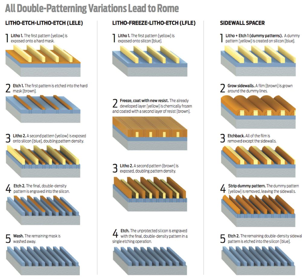
But double patterning is very difficult to implement practically. There are several impediments, which is why the technique comes in three major flavors, each of which offers its own benefits and drawbacks: litho-etch-litho-etch (LELE); its close cousin, litho-freeze-litho-etch (LFLE); and the sidewall-spacer technique.
 Emily Cooper
LELE is the most straightforward. As the name suggests, two complete lithography-and-etch operations are carried out, one atop another, to transfer the mask pattern to the wafer [see “The Two-Step”]. Think back to the dog and the fence: LELE is the closest analogue to simply buying two fences and stacking them one in front of the other. One big drawback of this approach is cost: two complete pattern-transfer operations will essentially double your lithographic cost, just as buying two fences would double your fence cost.
 The Two-Step: Three scanning electron microscope photos of different examples of LELE double patterning, each one showing the final result. The dark-colored features were printed in one lithography/ etch step, and the light-colored features in the second lithography/etch step.Photo: IMEC
Another problem is an extreme sensitivity to overlay accuracy. When the mask pattern is projected onto the wafer the second time, any variations in overlay—that is, misalignments between the placement of the second printed pattern with respect to the first—will translate into variations in the width of the spaces between the lines. In fence terms, it means you need to line your fences up so that every post is spaced exactly the same distance apart. If you make a mistake, for example shifting it by a third instead of half the pitch, your dog will be able to squeeze through every other gap.
Early results for LELE have been promising, but we need to improve the overlay capabilities of current exposure tools. To put it in some perspective, LELE for a 64-nm pitch will require a pattern placement accuracy of 2 to 3 nm over an exposed area bigger than 2 by 2 centimeters. That’s not a lot of room for error, especially because lithographers are accustomed to a much more generous error allowance for single patterning. The industry still needs to come up with major improvements in pattern-placement accuracy if it wants to make LELE produce a good yield of working chips. Otherwise the promising results will stay in academic papers and never make it to commercial production.
Double-patterning flavor number two, LFLE, was developed to address LELE’s cost issue. LFLE is a variation on LELE: after the first lithography step forms the patterns on the wafer’s photoresist, a chemical treatment of the resist “freezes” the pattern. Then, without etching or otherwise transferring the resist pattern into the substrate, technicians apply a second film of resist over the first pattern. Because of the freeze operation, that second coating of resist does not intermingle with the existing pattern. A second lithography exposure and development creates the second pattern while leaving the first pattern intact. Then a single etching operation transfers the compound pattern into the underlying substrate.
To use the fence analogy again, this is the equivalent of hammering the two fences together before you put them in the ground—saving time and money by putting only one fence into the ground instead of two. The fact that all these exposure and processing steps can be carried out within a single machine significantly reduces cost and processing when compared with LELE. Recent progress in various freeze processes is making this approach look very attractive, but results are still preliminary. It’s not yet clear whether the new freeze materials can be manufactured, and the overlay difficulties of LELE are just as severe for LFLE.
The third variation of double patterning, the sidewall-spacer technique, is attractive because it elegantly addresses the problem of tighter overlay requirements. This technique creates small lines around the outer edge of the original pattern, doubling the frequency of lines for a repeating pattern, but not in the same blunt-force way as LELE and LFLE.
Consider the picket fence again. In the sidewall-spacer approach, a fence is built with spaces that are twice as big as what you actually need. Then smaller posts are attached to both sides of each original post. Then you remove the original posts. Now you have twice as many of the new, smaller posts as you had originally, and they are all perfectly spaced. In both the LELE and LFLE processes, the errors in overlay translate into irregular and uneven patterns that will cause the chip to fail. By contrast, the sidewall-spacer process does the opposite, turning dimensional errors (irregular patterns) into overlay errors. But because it’s easier to control a pattern’s dimensions than its placement, the sidewall-spacer process significantly relaxes the requirements of the lithographic optical system.
The main problem with the sidewall-spacer approach is that it restricts every final feature (the final, skinny “fence post”) to the smallest possible dimensions rather than whatever size the chip designer happens to want. Further, these sidewall-formed lines necessitate a second and sometimes even third patterning step: that’s because they add extra material not only onto the sides of the original patterns but on the fronts and backs as well, creating patterns that look more like closed loops than straight lines. Obviously, that is not what the final chip design is supposed to look like, so the extra patterns must be removed separately, and once again, that creates added cost. The sidewall-spacer technique is much better suited to creating memory cells than logic cells, because the patterns for memory cells are much more regular than those for logic cells, which are essentially random.
ASML, Canon, and Nikon, which supply the tools for all flavors of double patterning, tend to like LELE and LFLE best, mainly because mainstreaming these techniques will probably mean that IC companies will have to buy a new generation of scanners to get tighter overlay performance. For the sidewall-spacer technique, IC companies may be able to use their existing tools. Applied Materials is pushing the sidewall-spacer technique because it involves processing steps that will be done on Applied Materials tools, thus giving the company more tool sales.
Because essentially no IC companies are major players in both memory and logic, the big logic companies (the IBM partnership companies, Intel, Sony, TI, Toshiba, and TSMC) will stick with LELE and LFLE, while the big memory companies (Hynix, Micron, Renesas, and Samsung) will likely use the sidewall-spacer technique.
In the end, all double-patterning techniques will require new chip-design tools capable of splitting an existing chip mask layout pattern into two separate sets of mask patterns. An error in just one feature could kill an entire device, so we need automated and nearly foolproof pattern splitting. The common practice of scaling down a design from the previous node will no longer work.
Supposedly, the first production tools for EUV will arrive in 2011. These tools will be able to achieve resolutions of about 25 nm, which means they’ll be able to usher in the 22-nm node (but see sidebar, “Why There Will Never Be an 8-nm Semiconductor Node”). That’s according to the current schedule, anyway. Many people, myself included, are skeptical. Sure, the tools will be capable of 25-nm resolution, and sure, they’ll arrive by 2011. But they won’t be production worthy: they won’t have enough throughput and yield to make them worth buying—especially because by then, double-patterning lithography will be in full swing, and using it to create 22-nm chips will be a lower risk at a lower cost.
In the end, double patterning is nobody’s idea of an ideal solution. The extra steps and complexities could double the cost of lithography layers, pushing chip-making costs up even while consumers continue to expect more for less. Again, double patterning is probably the worst alternative—except for all the others.