While graphene by itself has been generating enormous interest in both the research community and outside of it, what many are still missing is that we are in the midst of a two-dimensional material explosion that goes beyond just graphene.
Molybdenum disulfide (MoS2) is beginning to take center stage right behind graphene in the cast of 2-D materials that includes silicene (a single layer of silicon) and boron nitride. Nearly three years ago, MoS2 was revealed as a possible 2-D replacement for three-dimensional silicon in transistors.
Even though MoS2 had an advantage over graphene in that it has an inherent band gap, it was really first imagined as a complement to graphene in applications such as optoelectronics and energy harvesting, where thin, transparent semiconductors are required.
Now researchers at Northwestern have gone back to MoS2's complementary role and combined it with carbon nanotubes to create p-n heterojunction diode. The p-n junction forms the backbone of devices such as solar cells, light-emitting diodes, photodetectors, and lasers.
“The p-n junction diode is among the most ubiquitous components of modern electronics,” said Mark Hersam, director of the Northwestern University Materials Research Center, in a press release. “By creating this device using atomically thin materials, we not only realize the benefits of conventional diodes but also achieve the ability to electronically tune and customize the device characteristics. We anticipate that this work will enable new types of electronic functionality and could be applied to the growing number of emerging two-dimensional materials.”
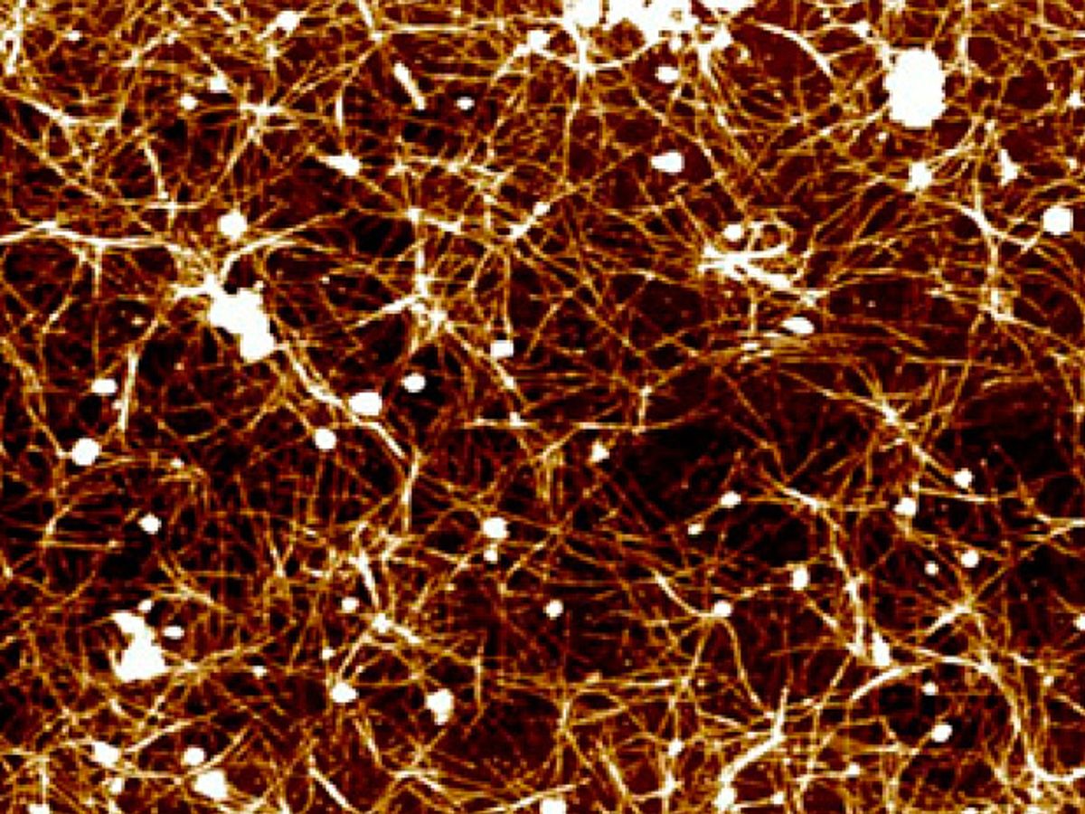
In a paper published in the journal Proceedings of the National Academy of Sciences (“Gate-tunable carbon nanotube–MoS2 heterojunction p-n diode”), the Northwestern team used single-walled carbon nanotubes as the p-type semiconductor and the MoS2 as n-type semiconductor.
The researchers discovered that when they stacked the two semiconductors vertically on top of each other they formed a heterojunction that allowed for the tuning of the device’s electrical characteristics with an applied gate bias.
In addition to its tunability, the p-n heterojunction diode is highly light sensitive. The researchers exploited this capability by making an ultrafast photodetector with the diode that displayed an electronically tunable wavelength response.
With 2-D materials already proving capable of making field-effect devices, it is hoped that this latest addition of a p-n junction diode made from one will mark an important step in the next generation of electronics.
Dexter Johnson is a contributing editor at IEEE Spectrum, with a focus on nanotechnology.


