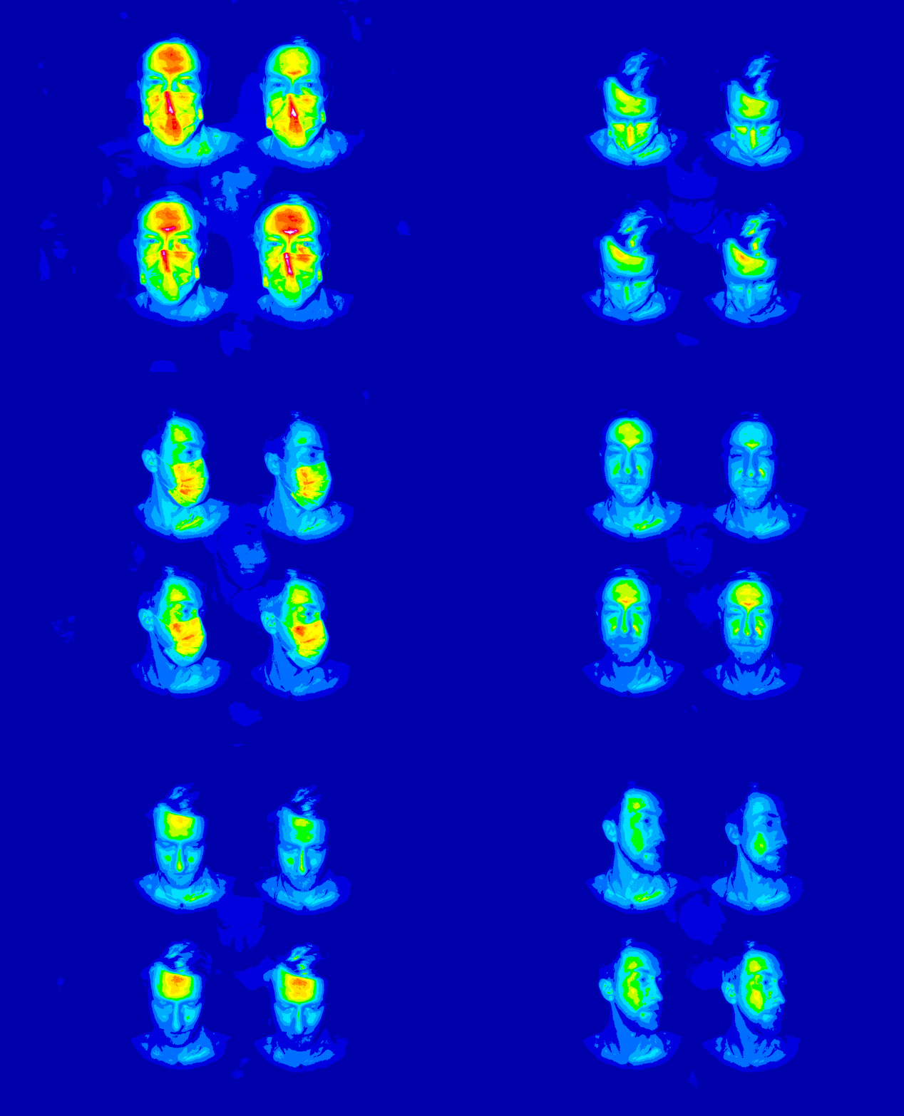
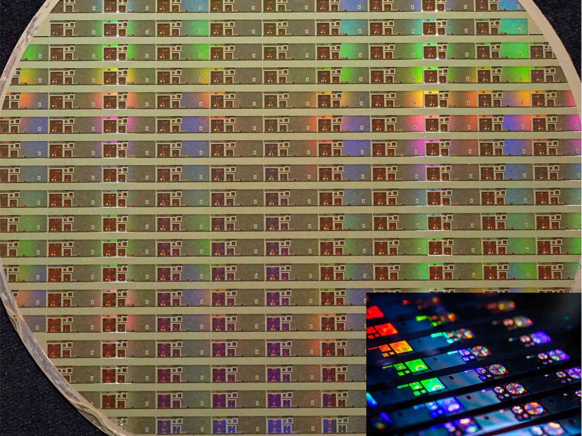
This week, startup Metalenz announced that it has created a silicon chip that, paired with an image sensor, can distinguish objects by the way they polarize light. The company says its “PolarEyes” will be able to make facial authentication less vulnerable to spoofing, improve 3D imaging for augmented and virtual reality, aid in telehealth by distinguishing different types of skin cells, and enhance driving safety by spotting black ice and other hard-to-see road hazards.
The company, founded in 2017 and exiting stealth a year ago, previously announced that it was commercializing waveguides composed of silicon nanostructures as an alternative to traditional optics for use in mobile devices.
Metalenz recently began a partnership with ST Microelectronics to move its technology into mass production and expects to be shipping imaging packages sometime in the second quarter of this year, according to CEO Robert Devlin.
IEEE Spectrum spoke with Devlin last week to find more about the company’s technology and what it will be able to do when it gets into consumer hands.
Before we talk about your new polarization optics, briefly help us understand how your basic technology works.
Robert Devlin: We use standard semiconductor lithography on 12-inch wafers to create nanostructures in the form of little pillars. These structures are smaller than the wavelength of light, so by changing the radius of the pillars, we can use them to control the length of the optical path of the light passing through. For the first generation of this technology, we are working with near-infrared wavelengths, which transmits through silicon, rather than reflecting as visible light would do.
What’s the advantage of using nanostructures over traditional lenses?
Devlin: Our technology is flat, for one. When you are using a curved lens to put an image on a flat sensor, you have to make all sorts of corrections using multiple lenses and finely controlling the spacing between the lenses to make it work; we don’t have to do that. We also can bring the functions of multiple traditional lenses onto one chip . And we can manufacture these lenses in the same semiconductor foundries as the image sensors and electronics used in camera modules.
The iPhone face ID system, for example, has three lenses: one diffractive lens, for splitting infrared light being projected onto your face into a grid of dots, and two refractive, for collimating the lasers to project onto the face. Some of these modules have an optical path that’s folded by mirrors, because otherwise they would be too thick to fit into compact spaces required for consumer devices. With the single-chip flat optics, we can shrink the overall thickness, and don’t need folded optical paths or mirrors in even the most space-constrained applications.
3D mapping is another infrared imaging application that uses multiple lenses today. Augmented reality systems need to create a 3D map of the world around them in real time, in order to know where to place the virtual objects. Today, these use a time-of-flight system—again, working in the infrared part of the spectrum—which sends out pulses of light and times how long they take to get back to the image sensor. This system requires several refractive lenses to focus the outgoing light and a diffractive lens to multiply the light to a grid of points. They also require multiple lenses on the imaging side to collect the light from the scene. Some of the lenses are needed to correct for the curvature of the lenses themselves, some are needed to make sure the image is crisp across the entire field of view. Using nanostructures, we can put all of these functions onto one chip.
So that’s what the chips you announced do?
Devlin: Yes, and the first product to use our technology, shipping in the second quarter of this year, will be a module for use in 3D imaging.
Initially for mobile phones?
Devlin: For consumer devices generally but also for mobile phones.
What about AR?
Devlin: Of course, everyone is eagerly waiting for AR glasses, and the form factor remains a problem. I think what we are doing—simplifying the optics—will help solve the form-factor problem. People get suspicious if they see a big camera sitting on someone’s face. Ours can be very small, and, for this application, infrared imaging is appropriate. It allows the system to understand the world around it in order to meld the virtual world with it. And it isn’t affected by changes in lighting conditions.
Okay, let’s talk about what you’re announcing now, the polarization technology, your PolarEyes.
Devlin: When we spoke a year ago, I talked about Metalenz wanting to not just simplify existing mobile-camera modules, but to take imaging systems that have been locked away in scientific laboratories because they are too expensive, complex, or big, and combine their optics into a single layer that would be small enough and cheap enough for consumer devices.
One of those imaging systems involves the polarization of light. Polarization is used in industrial and medical labs; it can be used to see where cancerous cells start and end, it can in many cases tell what material something is made of. In industry, it can be used to detect features of black objects, the shape of transparent objects, or even scratches on transparent objects. Today, complete polarization cameras measure around 100 by 80 by 80 millimeters, with optics that can cost hundreds of dollars.

Using metasurface technology, we can bring the size down to 3 by 6 by 10 mm and the price down to [US] $2 to $3. And unlike many typical systems today, which take multiple views at different polarizations sequentially and use them to build up an image, we can use one of our chips to take those multiple views simultaneously, in real time. We take four views—that turns out to be the number we need to combine into a normal image or to create a full map of the scene color-coded to indicate the complete polarization at each pixel.
Besides the medical and industrial uses you mentioned, why else are polarized images useful?
Devlin: When you get these into mobile devices, we will likely find all sorts of applications we haven’t thought of yet, and that’s really exciting. But we do have an initial application that we think will help get the technology adopted—that’s in facial recognition. Today’s facial recognition systems are foiled by masks. That’s not because they couldn’t get enough information from above the mask to recognize the user. They use a high-res 2D image that provides enough data to the algorithms to do that. But they also use a 3D imaging system that is very low resolution. It’s meant to make sure that you’re not trying to spoof the system with a mask or photograph, and that’s what makes facial recognition fail when you are wearing a mask. A polarization imaging module could easily distinguish between skin and mask and solve that problem.
- Inside the Development of Light, the Tiny Digital Camera That ... ›
- Metasurface Optics for Better Cellphone Cameras and 3-D Displays ... ›
- Can Silicon Nanostructures Knock Plastic Lenses Out of Cell Phone ... ›
- 3D Chip Tech Is Key to Meta’s AR Goals - IEEE Spectrum ›
Tekla S. Perry is a former IEEE Spectrum editor. Based in Palo Alto, Calif., she's been covering the people, companies, and technology that make Silicon Valley a special place for more than 40 years. An IEEE member, she holds a bachelor's degree in journalism from Michigan State University.


