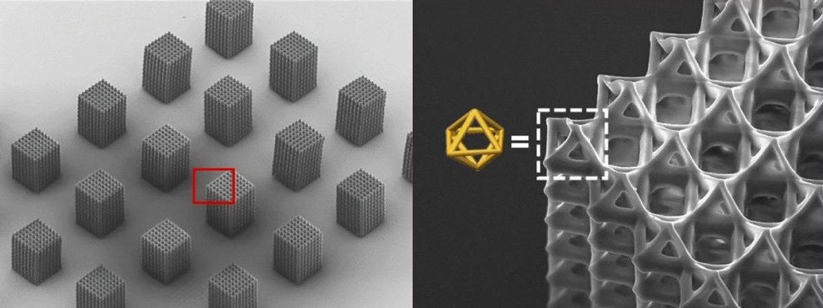
Using holograms, a nanoscale 3D printer can now rapidly fabricate complex items with details smaller than a wavelength of visible light, a new study finds. This research can rapidly manufacture nanotechnological arrays of wires, lenses, rotating magnetic gears, and other structures—suggesting applications in electronics, photonics, microrobotics and more.
Currently, the most precise 3D-printing technique for manufacturing nanoscale objects with complex shapes is likely two-photon lithography. This approach relies on liquid resins that solidify only when they absorb two photons of light at the same time instead of just one. This enables precise fabrication of items with voxels—the 3D equivalent of pixels—only a few dozen nanometers in size.
However, two-photon lithography has proven too slow and expensive for large-scale practical applications. This has largely rendered it an expensive laboratory tool to produce microscopic prototypes.
The new method can manufacture complex, microscopic 3D objects such as letters, numbers, rings, lenses, and gears that can be remotely controlled by applying a magnetic field.
Previous research has sought to split the laser beam used in two-photon lithography into multiple focal points to speed up fabrication. However, this strategy typically still achieves printing speeds of only about 10,000 voxels per second and less than 0.1 cubic millimeters per hour. Moreover, this approach is usually not able to control each individual laser’s focus, and so cannot produce highly variable structures.
Now a new two-photon lithography technique can print nanoscale 3D objects at speeds of up to 2 million voxels per second and 4.5 to 54 cubic millimeters per hour. In addition, it achieved a resolution of up to 90 nanometers, the best seen yet in high-throughput two-photon lithography, the scientists noted. Moreover, the team’s new process can simultaneously operate up to 2,000 individually programmable laser foci to fabricate complex structures, the most seen yet in high-throughput two-photon lithography, they added.
“The increase in throughput means the cost is substantially reduced, and the technology can now be used for industrial-scale applications at a more reasonable price and fabrication rate,” says study senior author Shih-Chi Chen, an optical scientist and mechanical engineer at the Chinese University of Hong Kong.
Solidifying the resin used in two-photon lithography requires extremely high laser intensities. Using multiple laser foci increases the laser power required, and the lasers typically used in two-photon lithography can barely provide the power needed to support more than 50 foci. In contrast, the new method used a near-infrared laser with a peak power of approximately 10 gigawatts.
Usually, two-photon lithography relies on foci that receive about 10,000 low-power laser pulses in order to fully solidify a voxel. However, the new technique uses a laser that fires tens to hundreds of thousands of times slower than the lasers typically used in two-photon lithography. To compensate, the new technique uses a single pulse to solidify each voxel. This required significant tinkering with the light-sensitive resin to optimize its printing quality, the scientists said.
“We achieved the best resolution with single-pulse exposure, which is totally opposite to the conventional approach to achieve high resolution—that is, low average power and long exposure time,” Chen says.
The new method fires a thousand 100-femtosecond-long pulses per second, bouncing these pulses off a digital micromirror device that displays a hologram. The scientists could use the hologram to divide each laser pulse into up to 2,000 foci with individually controllable strength, location and phase that could operate simultaneously in parallel.
In experiments, the researchers showed their new method could manufacture complex, microscopic 3D objects such as letters, numbers, rings, lenses, and eggbeater-like structures. They also fabricated magnetic gears they could remotely control by applying a magnetic field.

In the new study, the scientists also revealed they could modify the laser power of each focus to achieve 11 different intensity levels. This “gray-scale control” may find use in adjusting the solidity and mechanical properties of each voxel. The new technique displayed gray-scale control with an accuracy of more than 99 percent, the highest seen yet in parallel two-photon lithography, the scientists noted.
In addition, the researchers reported, the new method yields the highest energy efficiency yet in two-photon lithography. Whereas other techniques demand an operating power of roughly 1.5 to 4 watts, the new method requires only an average power of 400 milliwatts to operate 2,000 foci.
One potential application for nanoscale 3D printing is fabricating metastructures—materials whose structures possess repeating patterns at scales that are smaller than the wavelengths of whatever force they are designed to influence. Optical metastructures, which are designed to manipulate electromagnetic radiation, can bend light in unexpected ways, resulting in invisibility cloaks and other devices.
One of the greatest challenges with research into metastructures is manufacturing objects containing subfeatures less than a micrometer in size but, on the whole, are many thousands of times as large as their subfeatures. In experiments, the scientists revealed their new technique could fabricate a grid roughly 1 cubic millimeter in size made up of more than 680,000 cells with subfeatures as small as 700 nanometers.
The researchers are now exploring using AI to generate optimal fabrication procedures with their new technique. The aim is for the products to “have better structural integrity, strength, and uniformity,” Chen says.
The scientists detailed their findings online 27 March in the journal Nature Communications.
- 3D Bioprinter Prints Tissue in Situ - IEEE Spectrum ›
- The World's Largest 3D Metal Printer Is Churning Out Rockets - IEEE ... ›
- First 3-D-Printed Metal Gun Shows Tech Maturity - IEEE Spectrum ›
- The Practical Power of Fusing Photons - IEEE Spectrum ›
Charles Q. Choi is a science reporter who contributes regularly to IEEE Spectrum. He has written for Scientific American, The New York Times, Wired, and Science, among others.


