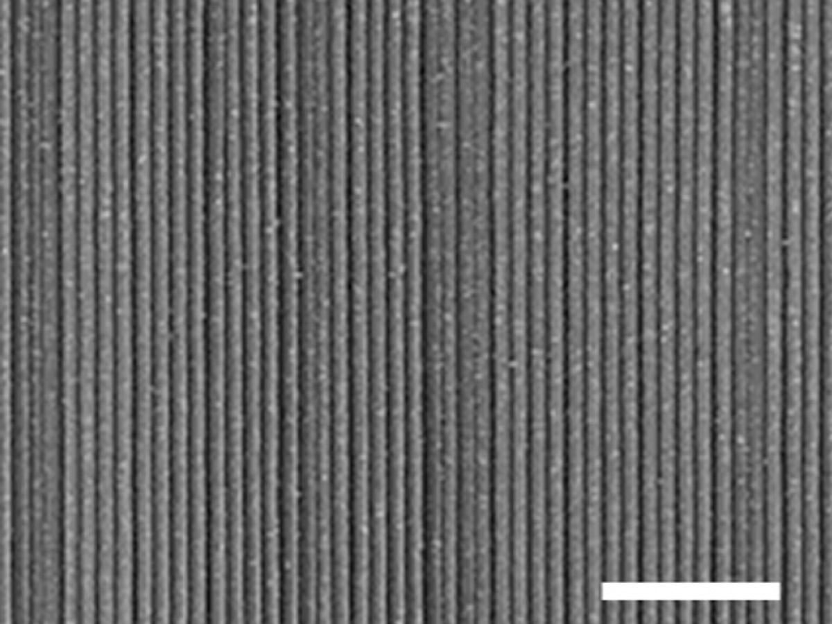
Nanowires don’t quite get the recognition that their high-profile nanomaterial cousins carbon nanotubes and graphene receive. But nanowires are quietly leading toward big improvements in a new generation of photovoltaics, plastic OLEDs (organic light-emitting devices), and a bunch of other applications.
Nanowires have suffered from the same manufacturing issues that other nanomaterials have endured, namely achieving large scale production while maintaining quality. One of the key problems nanowire developers have had to overcome is getting the nanowires to orient themselves in perfectly even arrays.
Researchers at the Korea Advanced Institute of Science and Technology (KAIST) in cooperation with LG Innotek have found a solution to that problem. And that solution moves away from traditional chemical synthesis to toward tricks common to semiconductor manufacturing.
In research published in the journal Nano Letters (“High Throughput Ultralong (20 cm) Nanowire Fabrication Using a Wafer-Scale Nanograting Template”), the Korean team leveraged semiconductor processes to produce highly-ordered and arrays of long (up to 20 centimeters) nanowires, eliminating the need for post-production arrangement.
The process involves a photo engraving technique on a 20-centimeter diameter silicon wafer. First the researchers created a template on the wafer consisting of an ultrafine 100-nanometer linear grid pattern. Then they used this pattern to lay down the nanowires using a sputtering process. The method produces nanowires in bulk in perfect shapes of 50-nm width and 20 cm maximum length.
“The significance is in resolving the issues in traditional technology, such as low productivity, long manufacturing time, restrictions in material synthesis, and nanowire alignment,” commented Professor Jun-Bo Yoon of KAIST in a press release. “Nanowires have not been widely applied in the industry, but this technology will bring forward the commercialization of high performance semiconductors, optic devices, and biodevices that make use of nanowires.”
Because the process doesn’t require a long synthesis time and results in perfectly aligned nanowires, the industrial partners in the research believe that it’s a technique that should lend itself to commercialization.
Image: KAIST
Dexter Johnson is a contributing editor at IEEE Spectrum, with a focus on nanotechnology.


