Researchers at Purdue University’s Birck Nanotechnology Center are turning toward two-dimensional materials as the future hope for meeting the demands of Moore’s Law.
The entire computer chip industry has long been engaged in a struggle to make sure that CMOS chips--which have been the cornerstone of computers for a generation--continue to perform well despite the challenges commensurate with the ever decreasing feature sizes demanded by Moore’s Law.
Intel changed the game two years ago when it introduced its 3-D dimensional transistor, essentially moving the gate that separates the drain and source into a perpendicular position with respect to the transistor plane. Some believe that this will satisfy Moore's Law's demands for the near future. But what happens when this latest architecture is no longer able to do the job?
The Purdue researchers believe that the answer is new materials beyond silicon.
"We are going to reach the fundamental limits of silicon-based CMOS technology very soon, and that means novel materials must be found in order to continue scaling," said Saptarshi Das, one of the Purdue researchers, in a press release. "I don't think silicon can be replaced by a single material, but probably different materials will co-exist in a hybrid technology."
Indeed, the competition for the two-dimensional material of the future that will replace silicon appears to be in full swing. Until recently, that competition had been between just graphene and molybdenum disulfide (MoS2), but just last week we reported on a new contender, germanane. Germanane is a one-atom thick layer of germanium. While both germanane and MoS2, with their intrinsic band gaps, have an advantage over graphene, germanane has an edge over MoS2: nearly a half-century of characterization and development of germanium for the chip industry.
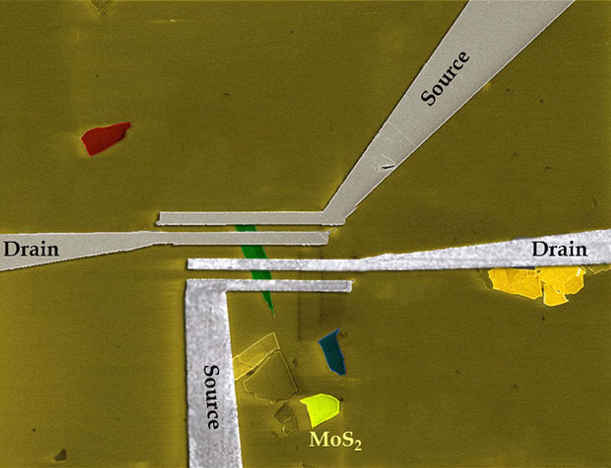
Nonetheless, the race has not been won yet. The Purdue researchers, including Joerg Appenzeller, a professor of electrical and computer engineering and scientific director of nanoelectronics at Purdue's Birck Nanotechnology Center, have sandwiched together 0.7-nanometer-thick strips of MoS2 into 15-ply sheets with a total thickness of 8 to 12 nanometers. But the main thrust of the work was not the fabrication of the 2-D material. Instead it was to look at carrier transport in the material. Their findings should shine a light on how layer thickness impacts field-effect mobility and in turn help the design of future chips. In their specific study, the researchers observed a non-monotonic trend in the extracted effective field-effect mobility with layer thickness.
Das and Appenzeller believe their research, which was published in the journal Rapid Research Letters ("Screening and interlayer coupling in multilayer "), provides a generic framework that will aid in the design and fabrication of any 2-D layered system.
This research has not yielded any clarity regarding which 2-D material will finally be the one that replaces silicon, but it does give the entire field of 2-D materials another design and characterization tool for making that day a more likely outcome for all of them.
Image: Birck Nanotechnology Center, Purdue University
Dexter Johnson is a contributing editor at IEEE Spectrum, with a focus on nanotechnology.


