Graphene is growing up (or, rather, out). When physicists Andre Geim and Konstantin Novoselov first isolated the speedy two-dimensional material in 2004 using sticky tape, they were lucky to create flakes of the stuff that spanned a few micrometers.
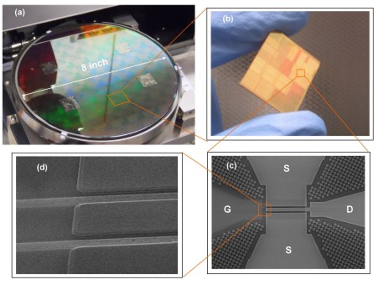
Now, IBM has demonstrated the ability to make integrated circuits on 200-mm wafers coated with a continuous layer of the atom-thick material. The results were reported on Monday at the 2011 International Electron Devices Meeting in Washington, D.C. According to a paper submitted to the conference by Shu-Jen Han of IBM’s T.J. Watson Research Center in Yorktown Heights, New York and colleagues, the demonstration is a “major step in transitioning this promising material from a scientific curiosity into a real technology.”
To create the large wafers, Han and colleagues grew graphene on copper foil from vapor heated to more than 900 degrees C. The team coated this graphene layer with the polymer PMMA and then dissolved away the copper, leaving a bottomless graphene layer that could be picked up and placed onto a silicon wafer.
Before placing the graphene on the wafer, the team etched in deep trenches and filled them with tungsten to create gates. The source and drain regions of each transistor, which are used to pass current through each graphene channel, were built on top of the graphene sheet.
IBM has previously declared an interest in wafer-scale processes, but until now it wasn’t quite clear how far along the research had progressed. Just a few months ago, the company published a paper reporting on a much smaller-scale development: the first integrated circuits made from graphene.
Like earlier devices, the graphene transistors that IBM has built are radio frequency (RF) devices, the sort that are used to build electronics such as digital signal processors. Because graphene has no natural bandgap, its electrons are always in some conductive state. Transistors built from the material can't be switched on and off to create logic. Researchers have a few different tricks that can be used to create a bandgap, but work on graphene-based RF devices is much farther along.
So when will we see graphene-based electronics fully emerge from the lab? All the devices on the wafer are functional, Han says, but “the variation is still pretty large and a lot of them will fall out of spec.” The culprit seems to be graphene quality. The team found that smaller devices on the wafer show better performance than larger devices. They attribute the difference to the fact that larger devices have a higher chance of being built atop a defect, such as a boundary between differently oriented graphene crystals or a wrinkle in the graphene layer created during the transfer process. Ironing those defects out and improving crystal purity may take a bit of time, but considering how far the material's come in less than 10 years, I won't be placing any bets on how long it will take.
Images: IBM/IEDM
Rachel Courtland, an unabashed astronomy aficionado, is a former senior associate editor at Spectrum. She now works in the editorial department at Nature. At Spectrum, she wrote about a variety of engineering efforts, including the quest for energy-producing fusion at the National Ignition Facility and the hunt for dark matter using an ultraquiet radio receiver. In 2014, she received a Neal Award for her feature on shrinking transistors and how the semiconductor industry talks about the challenge.


