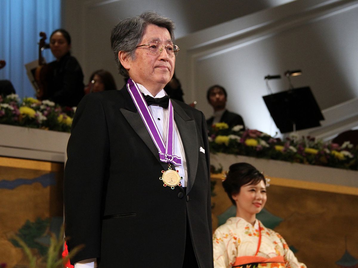
Takashi Mimura invented something wonderful in 1979. The high-electron-mobility transistor was intended as a device that can operate at microwave frequencies with ease. HEMTs are capable of fast switching because they confine the flow of current through a very-thin, high conductance layer called a two-dimensional electron gas. But it's the lack of noise in these transistors that really made their mark. They were integral to picking up the faint radio waves that carried Voyager 2’s photos of Neptune 1.3 billion kilometers to Earth in 1989, and now they’re in every satellite receiver you see. Mimura, a Fellow of the IEEE, won the coveted Kyoto Prize in 2017 for his efforts. He spoke to IEEE Spectrum through an interpreter on 21 March 2018.
IEEE Spectrum: In your words, what’s the difference between the HEMT and CMOS everybody sees?
Takashi Mimura: First of all, the major difference is the material. CMOS material is silicon. On the other hand, HEMT is a compound material like gallium arsenide or indium phosphide. For CMOS, it’s digital circuits—for example, a microprocessor or a memory IC. For HEMT, it's a single transistor for low noise. That’s the application.
Spectrum: What still excites you about HEMT research these days?
Mimura: What excites me about the HEMT research now is particularly in the material area. Traditionally [it was] gallium arsenide and indium phosphide. Now it’s expanding to different materials. This wasn’t possible in the past. That means we can use it for high frequency/high power and for power transistors. Which is a more economical application, so that’s what researchers are focusing on these days.
Spectrum: What other areas of semiconductor research do you find exciting?
Mimura: Lately, quantum computing is the focus. For elements for quantum computing, I’m looking at semiconductors. I believe for quantum computing, the manufacturability or technique is very important. Semiconductors have a long history of refining and enhancing manufacturing capability.
Spectrum: What do you think were the most unexpected uses of HEMTs?
Mimura: Initially to produce a HEMT was very expensive. So I did not expect HEMTs to be used for satellite broadcast antennas. That was a surprise. I did not expect that at all. The production cost has decreased to 1/10,000th [of the original cost], so now we can mass produce it. Now that production costs have become less expensive, satellite broadcast antennas incorporate HEMTs.
Programs are broadcast beyond country borders. In 1989, the Berlin Wall collapsed. A lot of people in eastern Germany were watching broadcast from western Germany. So in that sense, the HEMT had historical significance. Now everybody can have access to information beyond their borders. So in that way, the HEMT is providing borderless information.
Spectrum: What would you have done differently in your career?
Mimura: I’m interested in biology. And, of course, I’m interested in technology. So I would like to have studied some area in between biology and technology. The reason I’m saying that, is that when I was a child I was very much interested in insects. So perhaps that’s where this feeling comes from. I really liked reading the zoology of insects written by French writer [Jean-Henri] Fabre. I always wanted to live his lifestyle.
Samuel K. Moore is the senior editor at IEEE Spectrum in charge of semiconductors coverage. An IEEE member, he has a bachelor's degree in biomedical engineering from Brown University and a master's degree in journalism from New York University.


