
The frequency range of 10-100 GHz offers a gold mine of commercial and military applications. Full-blown system integration has been rare, however. Traditionally, microwave circuit designers interested in exploiting these frequencies have turned to discrete components, despite the expense of assembling and packaging them and the dearth of buyers that can afford the result.
Today this scenario is rapidly being transformed by indium phosphide heterojunction bipolar transistors (HBTs), a technology that is now yielding large-scale integrated (LSI) circuits packing 1000 to 10 000 transistors on a chip and operating at over 65 GHz. Success in integrating such fast, dense transistors has bred numerous analog, digital, and mixed-mode ICs having unprecedented performance. Moreover, such high-speed integration is not only possible but marketable, too, because consumer demand for data from the Internet, digital audio and video, and video-on-demand is on the rise.
In general, data is delivered to the consumer in two ways. Guided-wave propagation occurs along optical-fiber links and coaxial cables. Free space transmission is the territory of radio, television broadcasting, satellite links, local multipoint distribution systems, and wireless local-area networks.
For free space propagation, expensive installations are not necessarily required, but governments do regulate bandwidth and frequency use with a firm hand. As a result, new or large-bandwidth applications are forced to resort to unallocated higher carrier frequencies. For example, a new wireless local-area network may have to operate at 60 GHz. Besides possible economy, a second attraction of higher frequencies is that they use smaller antennas. Because antenna efficiency is proportional to carrier frequency, receivers of higher carrier frequencies need only compact antennas. An antenna just 10 cm in length suffices for collision avoidance automotive radar at 77 GHz, for instance.
As for guided-wave systems, cable has to be deployed, but once it is in place, bandwidth is relatively unregulated. In this kind of system (such as an optical-fiber data link), the development of high-frequency components is mainly a response to the call for higher data rates. As optical-fiber trunk lines are more fully exploited, the next generation of communications channels will come to operate at 40, 80, or 100 Gb/s, well above the current 2.5-10 Gb/s. In fact, 100-Gb/s links could be in production as soon as 2010.
These data rates raise another obstacle. The signals must be received and processed at high speed and then eventually slowed down to match silicon CMOS processing speeds of at best 1.5 Gb/s. Such a receiving circuit requires complexity at least at the LSI level.
Worth developing
The way things are tending, access to an ultrahigh-speed LSI technology will be a must for system designers. Happily, the necessary level of complexity and speed is available from HBT ICs built on indium phosphide substrates using materials with different energy bandgaps for the emitter, the base, and, sometimes, the collector. They are the only viable option today for ICs that require 30-GHz-plus frequencies and LSI complexity [Fig. 1].
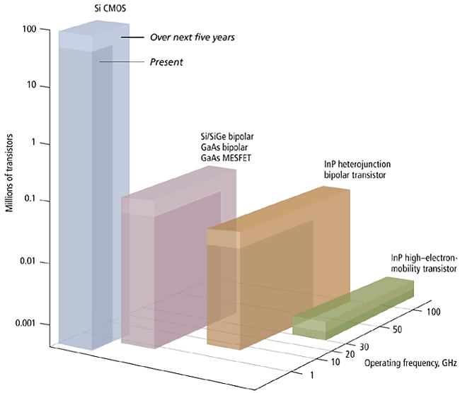 (1) Indium phosphide technology leads all others in operating frequency, but it is not expected to approach the integration scale of silicon chips. Silicon or silicon germanium (Si/SiGe) bipolar transistors and gallium arsenide (GaAs) bipolar transistors and metal semiconductor FETs (MESFETs) have intermediate combinations of speed and level of integration. The current state of the art (dark areas) can expect to improve over the next five years (light areas).
Applications that can get by with lower levels of integration but require higher frequency operation of 94 GHz and beyond, such as missile radar, are currently best served by indium phosphide high-electron-mobility transistors (HEMTs)—devices similar to depletion-mode field-effect transistors.
Indium phosphide transistors were first investigated in the early 1980s for their potential as optoelectronic communication devices. But a demonstration of an indium phosphide HBT IC was not reported until 1989, by a group at Rockwell Science Center in Thousand Oaks, Calif. Indium phosphide technology was originally funded through various U.S. government agencies interested in obtaining high-performance components for defense systems. Since then, the increased system throughput provided by these HBT ICs has encouraged a move toward commercial applications of the technology by such companies as TRW, Lucent, and HRL Laboratories in the United States and by Nortel in Canada. Research in indium phosphide monolithic microwave ICs and devices is also under way at many Japanese companies, including Hitachi, NEC, and NTT, and at many European research centers.
Currently the only obstacle to wider adoption of indium phosphide is the high cost of the 7.5-cm wafer substrate: it is about five times that of comparable gallium arsenide (GaAs).
Some material advantages
Indium phosphide is making its mark in bipolar transistors, rather than the field-effect transistors (FETs) found in most ICs. Of the two types, bipolar transistors are better suited to high-frequency operation. Their transconductance per unit length is higher, their device driving capabilities are better, and their device matching is superior. Because electrons move much faster than holes, high-speed bipolar transistors are usually npn in construction rather than pnp, relying on electron diffusion through the base and electron drift through the collector.
Bipolar ransistor speed is determined mostly by the time a charge-carrier (electron or hole) takes to pass through the device and the time the junction capacitances take to charge up. Thinner device layers, higher charge-carrier velocities, and higher current densities all increase frequency of operation, as do lower parasitic capacitances and lower device resistances.
Recognized metrics for the speed of transistors are the unity [see sidebar, "Defining Terms"], current gain cutoff frequency, f t , and unity power gain cutoff frequency, f max. The former is the frequency at which the current gain falls to one; f max is the highest frequency an oscillator made with a particular device can achieve. The first is strongly influenced by the minimum device dimensions in the direction of carrier flow and by device capacitances. The second is, on the other hand, quite sensitive to parasitic elements external to the core of the device, such as the transistor contacts. High values of both metrics are desirable for digital and analog design. While f t and f max values can be traded off against each other, balanced values are ideal for a general-purpose IC.
Normally, small gate lengths in MOS architectures or emitter widths in bipolar transistors lead to high cutoff frequencies. Compare NMOS, silicon germanium, and indium phosphide devices. NMOS devices with gate lengths of 0.18 µm have an f t of about 70 GHz and an f max of less than 40 GHz. The most advanced SiGe bipolar transistors have cutoff frequencies in the 80-100-GHz range. Indium phosphide HBTs having an emitter width of 0.5 µm, an f t over 250 GHz , and an f max over 1 THz (1000 GHz) have already been built by Mark Rodwell, at the University of California at Santa Barbara (UCSB). If such a device's depth were optimized and its emitter width could be scaled to dimensions used in current CMOS processes (about 0.2 µm), it would lead to a transistor with both f t and f max greater than 500 GHz.
As for high-electron-mobility transistors, indium phosphide devices with a 0.05-µm gate length have been demonstrated with 350-GHz f t and an f max above 800 GHz. But they are best suited for high-speed circuits at low levels of integration (less than 100 transistors). The gates of indium phosphide HEMTs must be written onto the chip using electron beams, because their horizontal dimensions are too small for photolithography techniques. Electron beam patterning of HEMTs can take days. These chips also show poor device matching, a major problem in integration. A comparison of various technologies must always take into account not only the speed but also the capability of producing complex circuits.
The frequency performance of HBTs can readily be tailored to suit designers' needs. It is done by growing different III-V semiconducting materials, one on top of the other, so as to engineer the transistors' bandgaps. This concept of a multiple-material HBT was described in William Shockley's original transistor patent (No. 2 569 347) issued in 1951. Only much later were the material structures that are now common contemplated and demonstrated: GaAs/AlGaAs in 1972, indium phosphide devices in 1982, and SiGe in 1987.
Mix and match
There are two versions of indium phosphide HBT, the single-heterojunction bipolar transistor (SHBT) and the double-heterojunction bipolar transistor (DHBT) [Fig. 2].
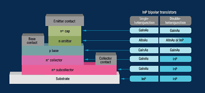 (2) Single- and double-heterojunction bipolar transistors (SHBTs and DHBTs, respectively) are made using a combination of materials, but start with an indium phosphide substrate. The ratio of gallium to indium in these transistors is 47:53, and the ratio of aluminum to indium is 48:52.
Both types of device allow for increased flexibility in the choice of transistor bandgaps, but a DHBT also improves on an SHBT's breakdown voltage.
The two device types are typically formed by creating the emitter from a wide-bandgap material such as aluminum indium arsenide (1.45 eV) or indium phosphide (1.35 eV) and the base from a narrower-bandgap compound, gallium indium arsenide (0.75 eV), for instance. A third material is used as the collector if the device is a DHBT or the same material is used for both collector and base in an SHBT.
This mix of materials has several advantages. For one, the bandgap of GaInAs, being narrower than that of silicon and GaAs, produces indium phosphide HBTs that have a very low turn-on voltage and are therefore ideal for low-voltage applications [Fig. 3, top left].
Another advantage is that the valence band offset, which blocks base-to-emitter hole flow, allows base doping to be one to two orders of magnitude higher in an HBT than in a single-material (homojunction) device. The effect is to lower base resistance, boosting f max and permitting smaller device dimensions. Typically the p-type base dopant is beryllium at a level of 2-5 x 10¹⁹ /cm3, the concentration being limited by the diffusivity of beryllium. But researchers at Bell Laboratories surpassed that limit in the mid-'90s. They succeeded in doping the base to 1020 /cm3 using carbon, an element that is all but immobile at the epitaxial growth temperatures for transistors.
Electrons move faster in both indium phosphide and GaInAs than in a silicon bipolar transistor [Fig. 3, lower left].
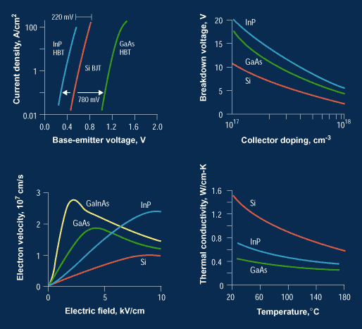 (3) A comparison of the material and electrical properties of silicon bipolar junction transistors (BJTs), indium phosphide heterojunction bipolar transistors (HBTs), and gallium arsenide (GaAs) HBTs indicates that indium phosphide and gallium indium arsenide (GaInAs) are superior in terms of current density, breakdown voltage, and electron velocity. These characteristics lead to low-voltage operation, improved power output, and higher frequency of operation respectively. But indium phosphide and GaAs lose out to silicon in terms of thermal conductivity.
Also, compared to silicon, for a given level of doping, indium phosphide has a high breakdown field. The breakdown field is a material property that helps determine the breakdown voltage of a device[Fig. 3, upper right]. Because of both characteristics, the designer can thin the collector layer and thus lower electron transit times. In contrast, when the collector in silicon (and SiGe) bipolar transistors is thinned to obtain higher speeds, breakdown voltages are unacceptably low for many applications. Figure 4 plots device breakdown voltage as a function of average cutoff frequency for various technologies and shows the advantage of choosing a material with a larger breakdown voltage for the collector.
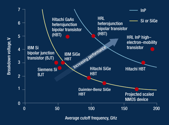 (4) Device breakdown voltage can be traded off for higher average cutoff frequency. For a given breakdown voltage, indium phosphide devices are faster than silicon, silicon germanium, and gallium arsenide devices.
Signal attenuation is also reduced when the substrate is indium phosphide. At higher frequencies the material inflicts less loss due to substrate resistance than does SiGe or silicon. However, like other III-V compounds and unlike silicon, indium phosphide is poor at conducting heat [Fig. 3, lower right]. To remove heat better from the compound semiconductor, the wafer must be thinned prior to packaging. Wafer thinning is also used for GaAs HBT chips that need to dissipate more than a few watts.
Many of the advantages mentioned apply to quite a few III-V materials. Still, indium phosphide HBTs are superior to, say, GaAs HBTs in some subtle but important ways. Take current gains. These are higher in indium phosphide HBTs with GaInAs bases, because carrier recombination at the outside surface of the base is 1000 times lower in GaInAs than in GaAs. This translates into an ability to scale indium phosphide HBTs to smaller horizontal dimensions than possible with GaAs HBTs, making for higher-speed ICs.
In addition, indium phosphide has a more versatile crystal size. It outdoes GaAs in the diversity of compounds whose crystal structures can be aligned, or lattice-matched, with its own structure. So a broad selection of device bandgaps, breakdown voltage, thermal conductivity, turn-on voltage, and electron velocity are available to the material. To illustrate, indium phosphide lattice-matched materials have a bandgap range of 0.7 to 2.1 eV, while GaAs-based materials range only from 1.4 to 2.2 eV.
Obviously, the wide array of materials that can work with indium phosphide powerfully favors its adoption as the substrate material of choice in high-speed applications. Laboratories around the world have used various combinations of these semiconductors to bandgap-engineer high-performance HBTs.
Fabricating the chip
The preferred method of increasing transistors' high-frequency performance is to shrink the devices. Generally speaking, the smaller the transistor, the shorter the distance electrons need to travel, and so the faster the device will switch.
In bipolar transistors, the critical dimensions are base and collector thickness, which are measured in tens of nanometers. They are realized by means of diffusion, ion implantation, or epitaxial growth—all of which are vertical processes that are controlled to nanometer precision.
The comparable FET dimension, gate length, is still measured in hundreds of nanometers. Only recently have advances in lithography tools allowed MOSFET gate length scaling to less than 200 nm—a feature size reached in bipolar transistors more than two decades ago. FET technologists have recently borrowed vertical fabrication techniques to create very short channels, but the new vertical FETs are still in their infancy.
In the most advanced of III-V bipolar transistors, the critical base layer is usually fabricated using molecular beam epitaxy (MBE) or chemical vapor deposition. Both techniques offer precise control of layer thickness, but both also generate wafer defects on the order of 100/cm2, several orders of magnitude larger than seen on an entire 200-mm silicon wafer. Defect densities arising during growth and processing are the major yield-limiters in indium phosphide HBT IC technology today.
Indium phosphide fabrication runs into the same sort of difficulties as GaAs processing, while also benefiting a great deal from the latter's two extra decades of development. A key issue here is that the substrates are neither as mechanically sturdy nor as resistant to chemical attack as is silicon. In addition, no native protective passivation layer akin to silicon dioxide exists for either GaAs or indium phosphide. Accordingly, the fabrication of those substrates has to take a different form than for silicon.
A GaAs or indium phosphide process also relies on etching to pattern the semiconductor layers that define the transistors. But the metal interconnects are handled by patterning, then deposition, and removal of unwanted metal by lift-off. This last step is a more benign process than etching, in that unwanted areas are simply floated off the substrate as the support layer beneath them is dissolved. Thin-film resistors, metal-insulator-metal capacitors, and interconnect lines are all formed in this manner to complete an IC, because use of etching would damage substrate layers.
A typical indium phosphide process employs successive etches to expose each of the three contacts of the transistor's stacked semiconductor layers. The emitter (on top) is first contacted (without etching), the first etch step stops on the base layer, the second etch step continues through the collector to the subcollector contact layer, and the final etch isolates adjacent transistors by removing the conductive subcollector layer.
It is a challenge to stop an etch uniformly, within a nanometer, across even a small (75- or 100-mm diameter) wafer. An elegant solution is to include etch-stop layers in molecular beam epitaxy growth, using material impervious to one etchant but easily removed by a second etchant. Indium phosphide etching thus involves a series of self-limited layer removals that result in atomically smooth surfaces for contacting the base and the collector.
The final device is typically much larger than the HBT, which is vertical, and also exceeds the total volume necessary for transistor action, which is only a few hundred nanometers deep and no more than 3 -m2 in area. The device requires the extra acreage to make contact with its neighbors and the outside world. These connections and the ensuing parasitic resistances and capacitances are responsible for most HBT performance limitations. Transistor theorists often refer to the contacting of the device as an "engineering" problem, as opposed to an issue of fundamental physical limits. Yet the fastest transistors and circuits are those that solve such engineering problems most effectively.
Parasitic problems
Numerous patents exist on processing techniques that minimize the effects of parasitic elements in silicon bipolar junction transistors and do so without modifying the intrinsic transistor. But these tricks add up to four extra lithography steps and up to 20 percent greater cost. III-V compound semiconductor processes, being relatively less mature, have had far less attention paid to their parasitic problems.
One major parasitic is the lateral resistances connecting the base, emitter, and collector of the HBT to their external contacts [Fig. 5].
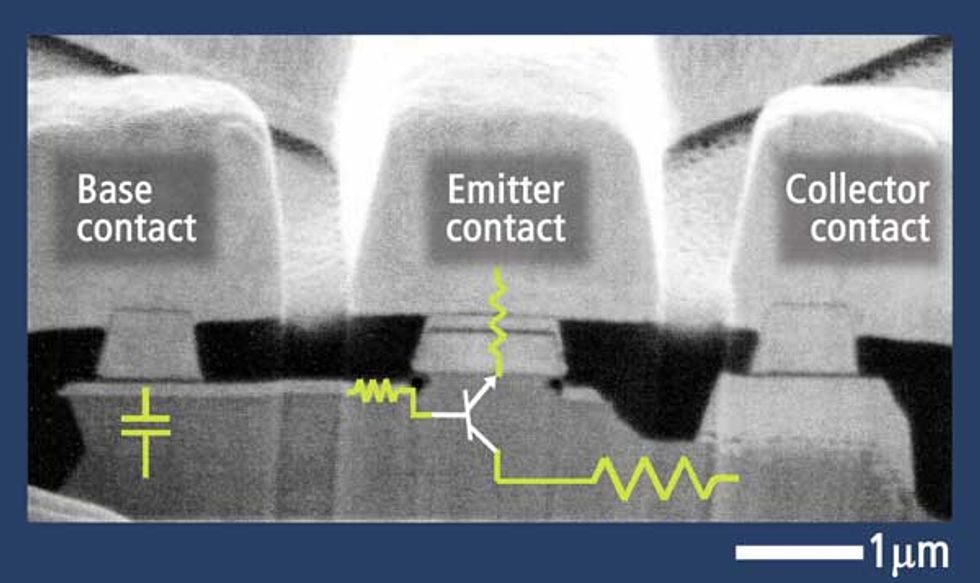 (5) Parasitic resistances and capacitances reduce the switching speed of the indium phosphide HBT. A scanning electron microscope shows their presence in the cross section of the 1-by-3-µm device.Photo: M. CASE, HRL LABORATORIES
The other is the vertical capacitance associated with base-collector overlap [Fig. 5, left lower corner]. Both parasitics grow larger as transistor layers are thinned to reduce electron transit time. Further shrinking of the device's horizontal dimensions is then required to reduce parasitic resistor lengths and parasitic capacitor areas. At the University of California at Santa Barbara, higher transistor speeds (specifically f max ) essentially are achieved by eliminating the parasitic base-collector capacitance.
Re-setting circuits
The indium phosphide HBT has provided record performance in recent years to a long list of circuits. Among them are power amplifiers, microwave monolithic ICs (MMICs), optoelectronic ICs, and LSI logic circuits.
Power amplifiers using indium phosphide double-heterojunction devices have shown power densities of over 2 W/mm of emitter length at 30 GHz with an efficiency of 35 percent. HBT MMICs include dc-to-85-GHz direct-coupled amplifiers and 108-GHz voltage-controlled oscillators. Multiplexing and demultiplexing circuits clocking at over 40 GHz with synchronous optical network (Sonet OC-768) capability have also been demonstrated.
One noteworthy indium phosphide record-setter is the static frequency divider. Also known as a prescaler, it is a divide-by-two circuit formed by feeding back the complementary output of a flip-flop to its input. The speed of this divider is often used to evaluate technologies because it represents the maximum clock rate for finite-state machines. Over the last couple of years, almost all record clock rates for static dividers have been established by indium phosphide HBT technology, which has a current maximum clock frequency of 66 GHz [Fig. 6].
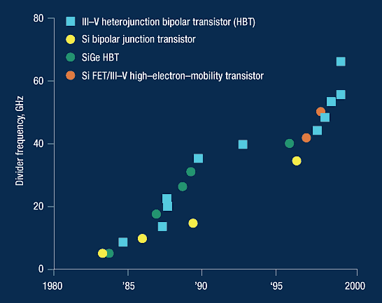 (6) Historically, heterojunction bipolar transistors (HBTs) made using indium phosphide or other III-V materials yielded the fastest static dividers.
Such HBTs not only yield the fastest circuits but also consume less power than other technologies, having the lowest power-delay product of any technology for 20-100-GHz operation [Fig. 7]. This achievement is owed to their lower turn-on voltage (the bandgap for GaInAs being smaller than for Si and GaAs) and a higher collector electron velocity. The combination allows indium phosphide HBT ICs to operate at clock frequencies up through 40 GHz with only 3-V power supplies.
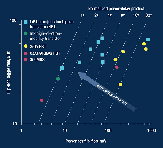 (7) For comparable speeds, indium phosphide flip-flops can consume as little as a tenth of the power of silicon-based devices. Diagonals represent lines of equal power-delay product.
Perhaps the most ambitious—and largest—single-chip indium phosphide system to date is a fiber-optic receiver that converts input light into digital data. The base-collector junction of an indium phosphide HBT serves as a photodiode. This chip takes 1.55-µm light input at 7.31 Gb/s and outputs digital data at a CMOS-compatible rate of 731 Mb/s. At lower integration levels, monolithic photoreceivers comprising a photodiode and a transimpedance amplifier—a photocurrent-to-voltage converter—with a bandwidth of 47 GHz have also been demonstrated. While 40-Gb/s transmitters and receivers have already been realized with indium phosphide HBT technology, 100-Gb/s receivers should be available in the next couple of years as device f t increases beyond 200 GHz.
A-D converters in the lead
Analog-to-digital converters (ADCs) helped motivate the initial development of indium phosphide HBT IC technology. Although fast devices in other technologies, such as HEMTs, were available, the lack of integration and poor device matching prevented the development of high-speed, high-resolution ADCs. With high-speed converters, system designers can move the analog-digital interface closer to the analog sensor and get nearer to realizing an all-digital system. To illustrate, a receiver that is all-digital at the sensor leads to a so-called software radio where numerous protocols and modulation schemes can be used without any hardware changes.
The fastest ADCs tend to be flash converters, which compare the indium phosphide input analog signal to 2n -1 equally-spaced reference voltages to produce an n-bit digital output. Flash ADC performance is limited by the speed and accuracy of the comparators (a circuit that compares two input voltages), which in turn depend on transistor f t and device matching—both strong points of indium phosphide devices. Suppose comparators are to operate at an error rate of 1 in a million samples at 20 GHz. That, to first order, would require a device f t in excess of 150 GHz. This speed requirement and the ability to integrate as many as eight matched comparators on a single IC spurred the advance of indium phosphide HBT technology. The fastest room-temperature monolithic ADC ever constructed was made at HRL Laboratories in 1994. A monolithic 8-gigasample-per-second, 3-bit flash converter, it used indium phosphide HBT technology and had an f t of about 100 GHz.
One-bit ADCs, also referred to as oversampled converters or delta-sigma converters, obtain high resolution, too. They use inaccurate analog components but sample at higher than the Nyquist rate of twice the signal bandwidth—hence the term "oversampled." In non-oversampled ADCs, the quantization noise (the error between the digitized signal and the input) is uniformly spread over all frequencies. But signal processing with an oversampled converter is combined with feedback from a low-resolution flash ADC to move the quantization noise out of the band of interest. A digital filter with a steep slope then processes the 1-bit data and eliminates the noise.
The key technology elements driving the realization of oversampled converters are a high transistor f t and adequate integration. The high f t increases sampling frequency and hence the resolution, and integration must be enough to slow down the 1-bit data stream so that it interfaces with a CMOS digital filter. In fact, high-resolution delta-sigma converters require device f t s in excess of 20 times the sampling frequency. Variations include converters that reduce quantization noise around dc—which is like a conventional ADC—or converters that reduce quantization noise about an intermediate frequency (IF).
Reducing quantization noise about an IF in a receiver has its advantages. It permits direct digitization of an incoming RF signal. There is no need to remove the carrier frequency or mix the signal down to baseband. Thus a receiver's power, weight, and cost can be reduced by getting rid of multiple mixers, filters, and phase shifters. An indium phosphide 1-bit bandpass delta-sigma converter that is sampling at 4 gigasamples per second has more than 13 bits of resolution over a 1-MHz bandwidth centered on an IF of 180 MHz. This performance is within a bit of the best baseband ADCs operating at 2 megasamples per second.
Still to be solved
Above and beyond the need for lower-priced indium phosphide wafers, the technology must leap a few technological hurdles before it can gain a wider welcome. While 100-Gb/s receivers are clearly on the horizon, a major problem exists in realizing 100-Gb/s transmitters. Laser driver amplifiers have conflicting requirements of high device breakdown voltages and high speed [see again Fig. 4]. Indium phosphide double-heterojunction bipolar transistors with f t beyond 150 GHz are adequate for 40-Gb/s links—but 100-Gb/s laser drivers remain a technology and design challenge.
Another challenge is that in order to use indium phosphide HBT technology for designs at clock rates beyond 20-30 GHz, an engineer must be familiar with both analog and microwave design techniques. Interconnect modeling has traditionally been the strong point of microwave designers, but the complexity of interconnects in an LSI chip makes many of their modeling techniques impractical. Conversely, the analog/digital design approach of modeling interconnects as resistor and capacitor combinations is also inadequate, because it does not include inductance and mutual inductance, which become important at high frequencies.
Going commerical
Problems of design will undoubtedly be overcome as the market for indium phosphide technology broadens. Driven by increasing consumer demand for data and other high-speed applications, indium phosphide-based HBT technology is currently in line to make the transition from military applications to commercial electronics over the next five years. The technology has already, and in a very short time, become the favorite for high-speed IC applications that need a frequency range of 10-100 GHz and require device matching and integration at LSI levels. As commercialization proceeds, lower substrate costs, higher integration levels, and lower production costs should bring about a dramatic increase in the use of indium phosphide HBT ICs in commercial high-performance systems.
To probe further
The latest circuit and technology results on indium phosphide-based heterojunction bipolar transistor (HBT) ICs can be found in the proceedings of two annual IEEE conferences: the International Conference on Indium Phosphide and Related Materials (IPRM), and the IEEE Gallium Arsenide IC Symposium. And dig into the Proceedings of the IEEE International Solid State Circuits Conference for a deeper understanding of the circuit issues discussed in this paper.
Indium Phosphide HBTs: Growth, Processing and Applications, edited by B. Jalali and S. J. Pearton (Artech House, Boston, 1995), is a comprehensive textbook on indium phosphide materials, devices, and circuits. Although most of the circuit results published in this book are no longer state of the art, it is a good starting point.
The Web site for the Federal Communications Commission (https://www.fcc.gov) is a good source of information on frequency allocation and applications such as local multipoint distribution service (27-30 GHz) and wireless ethernet (55-60 GHz).
A summary of the performance of over 170 published analog-to-digital converters fabricated in various technologies, including indium phosphide, can be found at https://www.hrl.com/micro/ADC/adc.html.
About the authors
Gopal Raghavan (M) is a principal engineer at Conexant Systems Inc., in Newbury Park, Calif., engaged in high-speed circuit design for optical networks. He has also worked at Intel Corp. and HRL Laboratories LLC in circuit design and process development.
Marko Sokolich (SM) is the manager of the integrated-circuit process engineering department at HRL Laboratories in Malibu, Calif., where he has been developing indium phosphide HBT processes for circuits with clock rates above 50 GHz. Prior to joining HRL in 1997, Sokolich was the program manager for magnetoresistor development and production at the Gallium Arsenide Operations of Hughes Aircraft Co.
William E. Stanchina (M) is the manager of the Microelectronics Laboratory at HRL Laboratories. He was one of the principal developers of the lab's InP HBT IC technology. Earlier, in 1984, he was on the electrical engineering faculty of the University of Notre Dame. He has served on the Indium Phosphide and Related Materials (IPRM) and International Electron Devices Meeting (IEDM) program committees and chaired the IEEE GaAs IC Symposium in 1998.