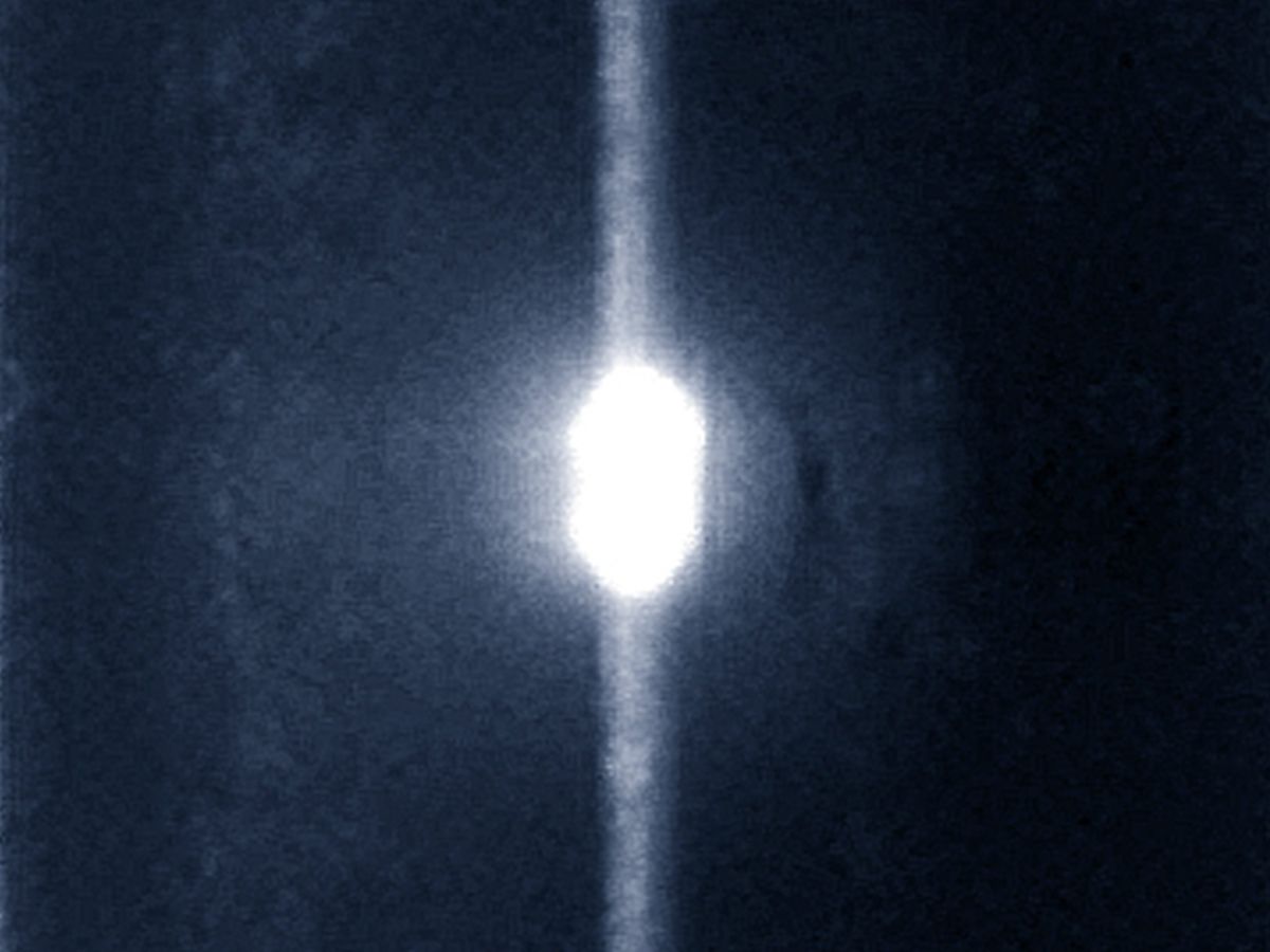
According to old-school physics, plasma shouldn't form in an electrified air gap smaller than about 5 micrometers. But it does. Nanoscale science still has some surprises in store, including a plasma-based device that engineers at Ecole Polytechnique Federale de Lausanne (EPFL) have now confirmed switches faster than anything we know of. In fact, they still don't really know how fast it switches, because the equipment doesn't exist that can measure it directly.
What engineers at EPFL have measured is a switch that can go from zero to 15.1 kilowatts in picoseconds. (A picosecond is one millionth of one millionth of a second, or about the time it takes light to travel one-third of a millimeter.) Even better, unlike any other device that can come close to this performance, the nanoplasma switch can be built on a chip with the other things you'd need for desirable circuits such as terahertz transmitters for future 6G cellular.
The nanoplasma switch is a simple, two-terminal device. It’s basically two metal electrodes on a substrate separated by a gap of air. Once the voltage across the gap crosses a particular threshold, charge leaps across and a conductive plasma forms. Exactly why plasma appears is still a bit of a mystery.
In an air gap much larger than 5 micrometers, plasma forms when an electric field accelerates an electron, which then smashes into a gas molecule, freeing more electrons, which accelerate and smash some more, eventually swelling into an avalanche of current. But things don’t work like that at shorter distances. An electron’s “mean free path” in air is about 5 micrometers. That means, on average, an electron will run into a molecule only every 5 micrometers of its journey.
“These devices work far below the mean free path in air,” says Mohammad Samizadeh Nikoo, a graduate student in the laboratory of Elison Matioli. Across such a small gap, tons of electrons are traveling ballistically, that is without interference that could resist or deflect them. “There is little interaction between the hot electrons and air,” he says.
In research reported this month in IEEE Electron Device Letters, Nikoo, Matioli, and colleagues tested the nanoplasma switch’s capabilities in “pulsed-power” applications. These are situations where you need to deliver a huge but practically instantaneous burst of power rather than a steady flow. That’s useful in things like triggering a nuclear bomb, firing a rail gun, or reversibly opening holes in cells to deliver therapeutics. The EPFL team embedded switches with gaps as small as 5 micrometers in an impulse generating circuit. They measured voltage rising as quickly as 14 kilovolts per nanosecond, putting out 870 volts with a peak current of 17.4 amperes for a power of 15.1 kilowatts.

Beyond pulsed power applications, it’s the chip-scale nature of the switch that is one of its most important aspects. Circuits such as terahertz transmitters and ultra-wideband emitters lose efficiency due to parasitic capacitance and inductance in the circuit board connecting their components. If those can instead be integrated on a chip, those parasitics would disappear. Because the nanogap switch is just metal on an insulator, it can be integrated on a chip with other components such as an antenna.
In research reported last year in Nature, the EPFL team did just that, integrating a switch with a bowtie-shaped antenna to generate near terahertz (109-GHz) signals. Samizadeh Nikoo and Matioli say they are working on demonstrating mass-production-ready all-metal integrated systems.
You could argue that if chip-scale integration is what you’re after, maybe going with a semiconductor switch would be better. But nanoplasma tech “is way faster than any typical semiconductor device,” says Matioli. Semiconductor switches have a fundamental switching speed limit of about 1 volt per picosecond, due to a combination of capacitance, maximum electron velocity, and critical electric field strength. But EPFL measured nanoplasma switches capable of at least 12 volts per picosecond.
Directly measuring just how fast nanoplasma switches work might not happen for a while. The nanoplasma speed records were made when engineers from Keysight brought a 110 GHz demonstration oscilloscope to Matioli’s lab for three hours. But even that instrument isn’t fast enough.
“We measured 5 picoseconds. But it could be 1 picosecond or 100 femtoseconds” or faster, says Samizadeh Nikoo.
Samuel K. Moore is the senior editor at IEEE Spectrum in charge of semiconductors coverage. An IEEE member, he has a bachelor's degree in biomedical engineering from Brown University and a master's degree in journalism from New York University.


