
Engineers in California have made an important advance in a technique that could help chipmakers create denser and cheaper integrated circuits. It might also extend the life of the traditional lithography process. With a method called directed self-assembly, the engineers were able to pattern contact holes for transistors in memory and logic circuits.
Today’s chips are made using lithographic tools that expose photosensitive materials to light with a 193-nanometer wavelength. But this approach has become increasingly challenging, especially when it comes to making the holes in which the electrical contacts to transistors are formed. Currently, holes are created from the intersection of two etched lines, a process that typically requires two separate lithographic steps and has become increasingly inaccurate as chip features have shrunk. State-of-the-art logic chips now require that holes be placed as little as 60 nm apart.
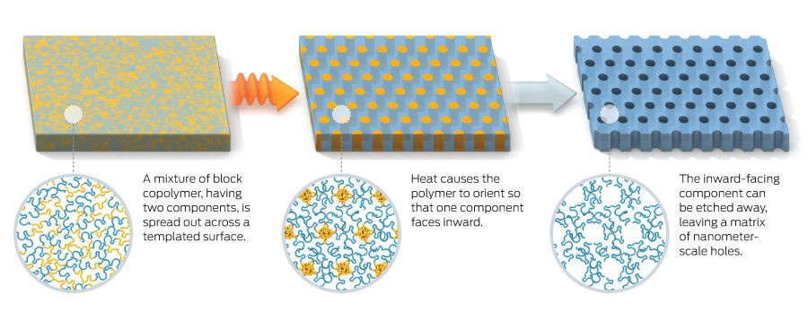
Directed self-assembly, which harnesses the ability of some molecules to rearrange themselves into ordered, nanometer-scale structures, has long been eyed as a way to make smaller features. But the process doesn’t naturally lend itself to chip designs, in which transistors and contacts are placed at varying distances. Molecules that self-assemble tend to form highly regular and extended arrays of alternating lines or tiled configurations of close-packed circles.
A group led by H.-S. Philip Wong, an electrical engineering professor at Stanford University, has found a way around this limitation by using ordinary lithographic methods to carve indentations that can act as guiding templates for smaller self-assembled features.
The team coated the entire surface of the silicon with a copolymer, each molecule of which consisted of a string of polystyrene linked to a string of poly(methyl methacrylate), or PMMA. When heat was applied, the PMMA side of each chain was drawn to other PMMA chains, balling together to form vertical cylinders within a matrix of polystyrene. Dissolving the PMMA left a polystyrene surface with holes that could be filled with conductive material to form electrodes. Successive etching steps left holes only where the indentations had been.
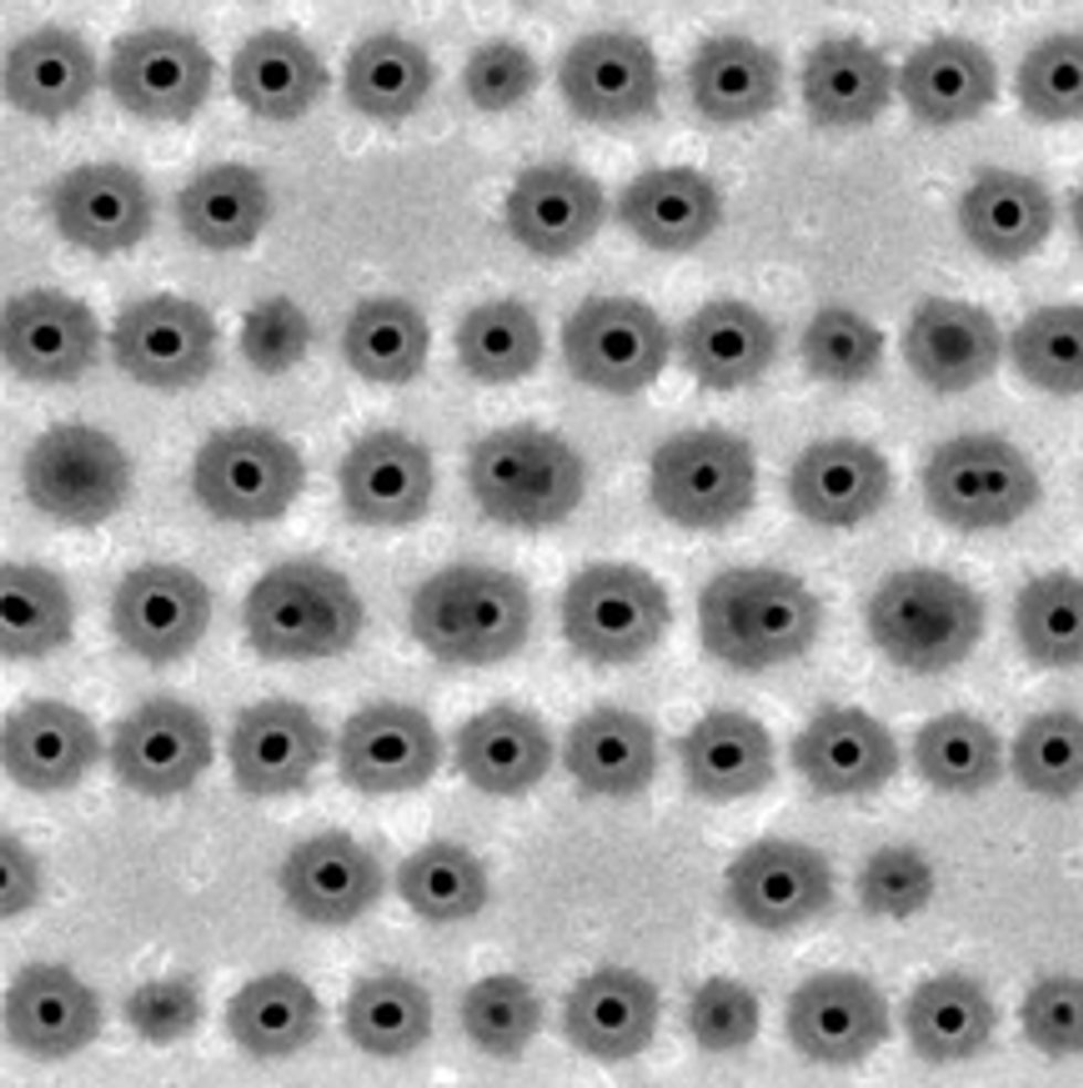
At the December IEEE International Electron Devices Meeting, in Washington, D.C., Xin-Yu Bao, formerly a postdoctoral researcher in Wong’s lab, showed that these small indentations could be used to reproduce a design for a memory circuit, an IBM 22-nm static RAM. Wong says the demonstration puts directed self-assembly in the running to compete with long-delayed, next-generation lithography tools, which use extreme ultraviolet light (EUV) to create patterns. Directed self-assembly ”can do what EUV can do, without the [US] $100 million investment,” says Wong.
At the SPIE Advanced Lithography symposium in San Jose, Calif., this month, Wong’s team will show that their template technique can pattern holes for a broad range of logic circuits, including adders and flip-flops, using a standard library of circuit components. These designs require simple indentations capable of holding one or two holes. But by altering the shape and size of the guiding templates, Wong says he expects to be able to create close-packed holes in squares, L ’s, T ’s, and other configurations. He believes that this alphabet of shapes will enable chipmakers to drive holes even closer together than can be accomplished with conventional lithography.
A number of other research groups are working on different aspects of directed self-assembly. ”What Stanford has done is to take all those ingredients and bake a pie,” says Chris Bencher, who is a member of the technical staff at Applied Materials and has collaborated with Wong’s group.
But Bencher notes there are two ways to make arbitrary patterns with directed self-assembly. One is to pattern small troughs, as Wong’s group has done. The other is to create a regular array of self-assembled structures and then eliminate the ones that aren’t needed. He suspects that Wong’s technique, which will require fewer steps, might be the first to make its way into industrial semiconductor manufacturing but that the latter method may ultimately be better suited to driving down the distance between holes.
Whichever strategy is adopted, researchers must still work to reduce the rate of defects from factors like impurities in the polymer. Bencher and his colleagues have found that roughly one out of every 25 million holes is missing. That’s a low rate, but it’s still too high to meet the exacting standards of the chip industry, whose ICs have upward of a billion contacts. But, says Bencher, ”we are definitely getting close.”
One application where directed self-assembly is likely to make its first inroads into industry is in hard-disk drives, which are considerably more tolerant of defects than chips are. The bits in hard disks are made out of grains of magnetic material, but these bits can't be made much smaller without greatly boosting the error rate. "We are definitely running out of gas," says Thomas Albrecht, who manages patterned media technology at Hitachi Global Storage Technologies, in San Jose. Within a few years, he says, "our progress with conventional media may slow to a crawl."
To keep shrinking bits, hard-disk makers are exploring ways to use self-assembly to make smaller bits for a master template that can be stamped onto wafers to create disks. At the SPIE meeting, Hitachi will show off a strategy for creating bits separated by a center-to-center distance of just 13.5 nm, a scale that should be suitable for hard drives more than twice as dense as today's state-of-the-art disks. But Albrecht says there are still quite a few hurdles that must be overcome before the technology can enter production.


