The Conversation (0)
edmon de haro
Purple
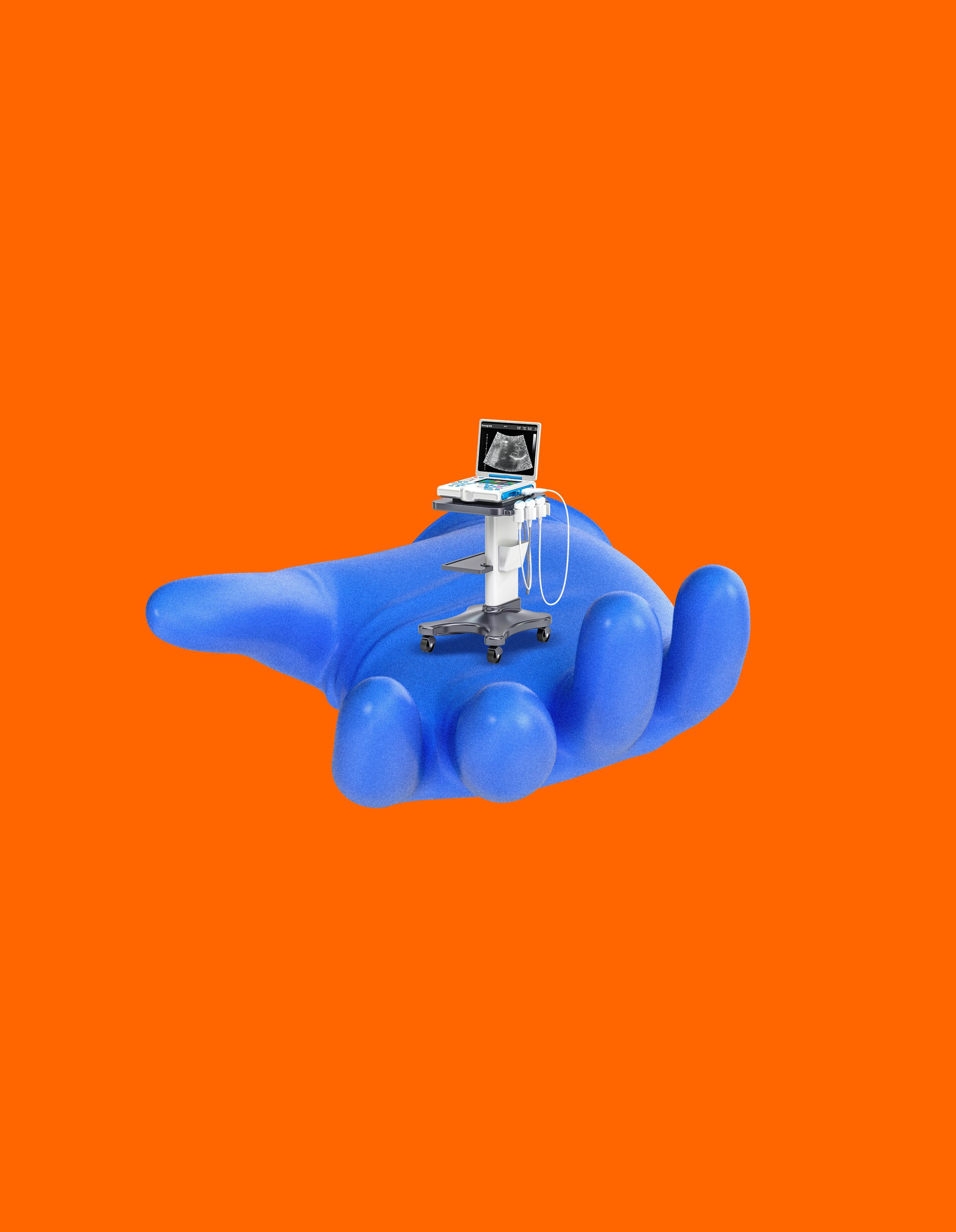
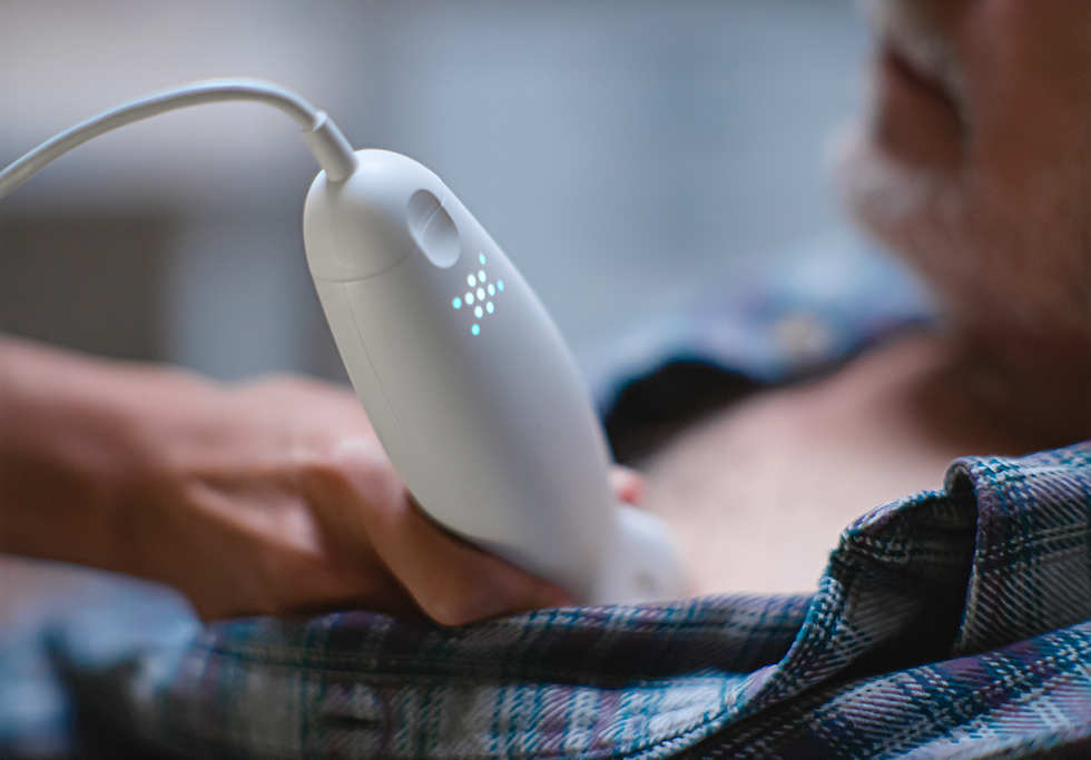
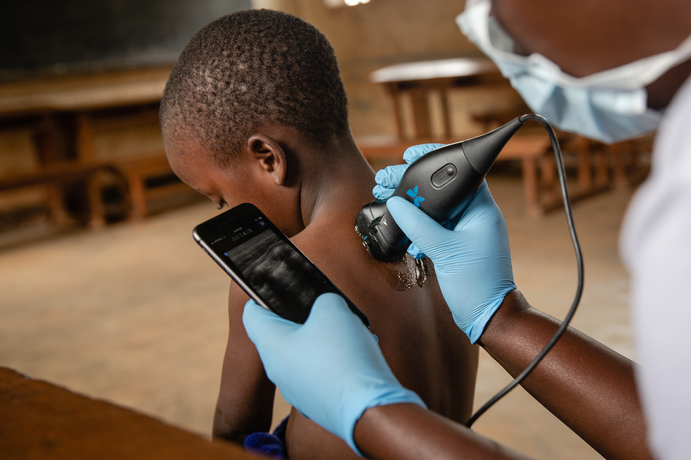
A startling change in medical ultrasound is working its way through hospitals and physicians’ offices. The long-standing, state-of-the-art ultrasound machine that’s pushed around on a cart, with cables and multiple probes dangling, is being wheeled aside permanently in favor of handheld probes that send images to a phone.
These devices are small enough to fit in a lab coat pocket and flexible enough to image any part of the body, from deep organs to shallow veins, with sweeping 3D views, all with a single probe. And the AI that accompanies them may soon make these devices operable by untrained professionals in any setting—not just trained sonographers in clinics.
The first such miniaturized, handheld ultrasound probe arrived on the market in 2018, from Butterfly Network in Burlington, Mass. Last September, Exo Imaging in Santa Clara, Calif., launched a competing version.
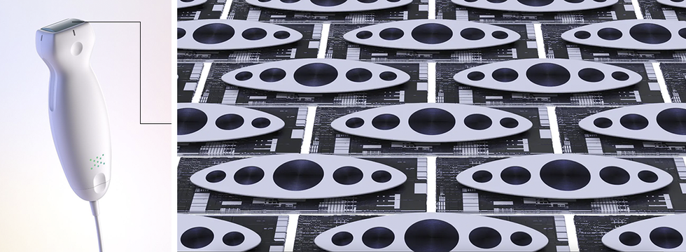
Making this possible is silicon ultrasound technology, built using a type of microelectromechanical system (MEMS) that crams 4,000 to 9,000 transducers—the devices that convert electrical signals into sound waves and back again—onto a 2-by-3-centimeter silicon chip. By integrating MEMS transducer technology with sophisticated electronics on a single chip, these scanners not only replicate the quality of traditional imaging and 3D measurements but also open up new applications that were impossible before.
How does ultrasound work?
To understand how researchers achieved this feat, it’s helpful to know the basics of ultrasound technology. Ultrasound probes use transducers to convert electrical energy to sound waves that penetrate the body. The sound waves bounce off the body’s soft tissue and echo back to the probe. The transducer then converts the echoed sound waves to electrical signals, and a computer translates the data into an image that can be viewed on a screen.
Conventional ultrasound probes contain transducer arrays made from slabs of piezoelectric crystals or ceramics such as lead zirconium titanate (PZT). When hit with pulses of electricity, these slabs expand and contract and generate high-frequency ultrasound waves that bounce around within them.
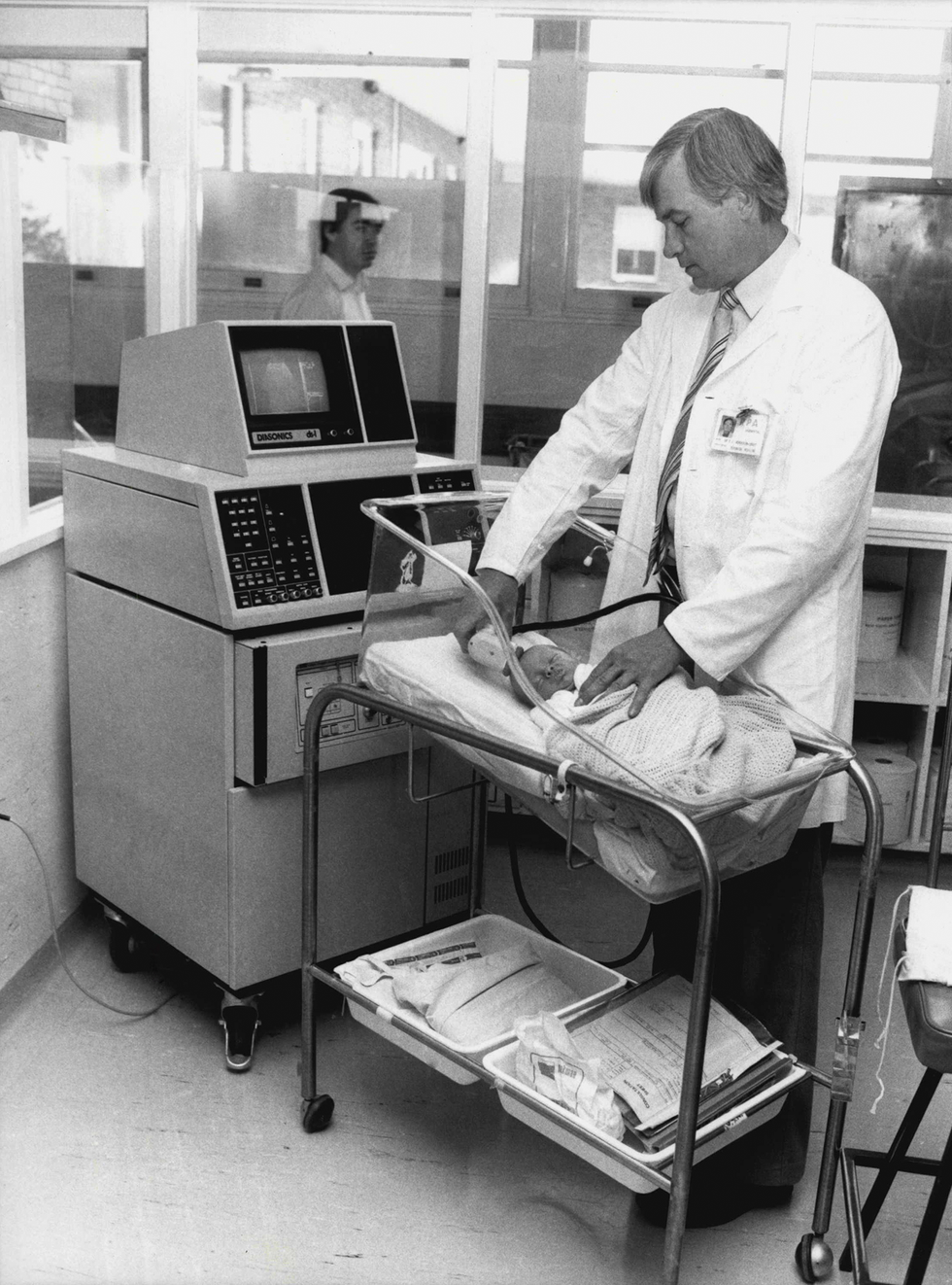 Ultrasound technology has historically required bulky machinery with multiple probes. Julian Kevin Zakaras/Fairfax Media/Getty Images
To be useful for imaging, the ultrasound waves need to travel out of the slabs and into the soft tissue and fluid of the patient’s body. This is not a trivial task. Capturing the echo of those waves is like standing next to a swimming pool and trying to hear someone speaking under the water. The transducer arrays are thus built from layers of material that smoothly transition in stiffness from the hard piezoelectric crystal at the center of the probe to the soft tissue of the body.
The frequency of energy transferred into the body is determined mainly by the thickness of the piezoelectric layer. A thinner layer transfers higher frequencies, which allow smaller, higher-resolution features to be seen in an ultrasound image, but only at shallow depths. The lower frequencies of thicker piezoelectric material travel further into the body but deliver lower resolutions.
As a result, several types of ultrasound probes are needed to image various parts of the body, with frequencies that range from 1 to 10 megahertz. To image large organs deep in the body or a baby in the womb, physicians use a 1- to 2-MHz probe, which can provide 2- to 3-millimeter resolution and can reach up to 30 cm into the body. To image blood flow in arteries in the neck, physicians typically use an 8- to 10-MHz probe.
How MEMS transformed ultrasound
The need for multiple probes along with the lack of miniaturization meant that conventional medical ultrasound systems resided in a heavy, boxy machine lugged around on a cart. The introduction of MEMS technology changed that.
Over the last three decades MEMS has allowed manufacturers in an array of industries to create precise, extremely sensitive components at a microscopic scale. This advance has enabled the fabrication of high-density transducer arrays that can produce frequencies in the full 1- to 10-MHz range, allowing imaging of a wide range of depths in the body, all with one probe. MEMS technology also helped miniaturize additional components so that everything fits in the handheld probe. When coupled with the computing power of a smartphone, this eliminated the need for a bulky cart.
The first MEMS-based silicon ultrasound prototypes emerged in the mid-1990s when the excitement of MEMS as a new technology was peaking. The key element of these early transducers was the vibrating micromachined membrane, which allowed the devices to generate vibrations in much the same way that banging on a drum creates sound waves in the air.
 Exo Imaging developed a handheld ultrasound machine using piezoelectric micromachined ultrasonic transducer (PMUT) technology.Exo Imaging
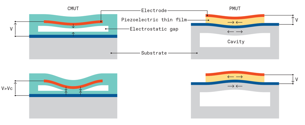
Two architectures emerged. One of them, called the capacitive micromachined ultrasonic transducer, or CMUT, is named for its simple capacitor-like structures. Stanford University electrical engineer Pierre Khuri-Yakub and colleagues demonstrated the first versions.
The CMUT is based on electrostatic forces in a capacitor formed by two conductive plates separated by a small gap. One plate—the micromachined membrane mentioned before—is made of silicon or silicon nitride with a metal electrode. The other—typically a micromachined silicon wafer substrate—is thicker and more rigid. When a voltage is applied, placing opposite charges on the membrane and substrate, attractive forces pull and flex the membrane toward the substrate. When an oscillating voltage is added, that changes the force, causing the membrane to vibrate, like a struck drumhead.
When the membrane is in contact with the human body, the vibrations send ultrasound frequency waves into the tissue. How much ultrasound is generated or detected depends on the gap between the membrane and the substrate, which needs to be about one micrometer or less. Micromachining techniques made that kind of precision possible.
The other MEMS-based architecture is called the piezoelectric micromachined ultrasonic transducer, or PMUT, and it works like a miniaturized version of a smoke alarm buzzer. These buzzers consist of two layers: a thin metal disk fixed around its periphery and a thin, smaller piezoelectric disk bonded on top of the metal disk. When voltages are applied to the piezoelectric material, it expands and contracts in thickness and from side to side. Because the lateral dimension is much larger, the piezo disk diameter changes more significantly and in the process bends the whole structure. In smoke alarms, these structures are typically 4 cm in diameter, and they’re what generates the shrieking sound of the alarm, at around 3 kilohertz. When the membrane is scaled down to 100 μm in diameter and 5 to 10 μm in thickness, the vibration moves up into megahertz frequencies, making it useful for medical ultrasound.
Honeywell in the early 1980s developed the first micromachined sensors using piezoelectric thin films built on silicon diaphragms. The first PMUTs operating at ultrasound frequencies didn’t emerge until 1996, from the work of materials scientist Paul Muralt at the Swiss Federal Institute of Technology Lausanne (EPFL), in Switzerland.
Early years of CMUT
A big challenge with CMUTs was getting them to generate enough pressure to send sound waves deep into the body and receive the echoes coming back. The membrane’s motion was limited by the exceedingly small gap between the membrane and the substrate. This constrained the amplitude of the sound waves that could be generated. Combining arrays of CMUT devices with different dimensions into a single probe to increase the frequency range also compromised the pressure output because it reduced the probe area available for each frequency.
 Butterfly Network developed a handheld ultrasound machine using capacitive micromachined ultrasonic transducer (CMUT) technology.Butterfly
The solution to these problems came from Khuri-Yakub’s lab at Stanford University. In experiments in the early 2000s, the researchers found that increasing the voltage on CMUT-like structures caused the electrostatic forces to overcome the restoring forces of the membrane. As a result, the center of the membrane collapses onto the substrate.
A collapsed membrane seemed disastrous at first but turned out to be a way of making CMUTs both more efficient and more tunable to different frequencies. The efficiency increased because the gap around the contact region was very small, increasing the electric field there. And the pressure increased because the large doughnut-shaped region around the edge still had a good range of motion. What’s more, the frequency of the device could be adjusted simply by changing the voltage. This, in turn, allowed a single CMUT ultrasound probe to produce the entire ultrasound frequency range needed for medical diagnostics with high efficiency.
Inside Butterfly Network’s CMUT ultrasound probe, the membrane collapses onto the substrate, generating an acoustic wave.Butterfly Network
From there, it took more than a decade to understand and model the complicated electromechanical behavior of CMUT arrays and iron out the manufacturing. Modeling these devices was tricky because thousands of individual membranes interacted in each CMUT array.
On the manufacturing side, the challenges involved finding the right materials and developing the processes needed to produce smooth surfaces and a consistent gap thickness. For example, the thin dielectric layer that separates the conductive membrane and the substrate must withstand about 100 volts at a thickness of 1 μm. If the layer has defects, charges can be injected into it, and the device can short at the edges or when the membrane touches the substrate, killing the device or at least degrading its performance.
Eventually, though, MEMS foundries such as Philips Engineering Solutions in Eindhoven, Netherlands, and Taiwan Semiconductor Manufacturing Co. (TSMC), in Hsinchu, developed solutions to these problems. Around 2010, these companies began producing reliable, high-performance CMUTs.
Early development of PMUTs
Early PMUT designs also had trouble generating enough pressure to work for medical ultrasound. But they could bang out enough to be useful in some consumer applications, such as gesture detection and proximity sensors. In such “in-air ultrasound” uses, bandwidth isn’t critical, and frequencies can be below 1 MHz.
In 2015, PMUTs for medical applications got an unexpected boost with the introduction of large 2D matrix arrays for fingerprint sensing in mobile phones. In the first demonstration of this approach, researchers at the University of California, Berkeley, and the University of California, Davis, connected around 2,500 PMUT elements to CMOS electronics and placed them under a silicone rubberlike layer. When a fingertip was pressed to the surface, the prototype measured the amplitudes of the reflected signals at 20 MHz to distinguish the ridges in the fingertip from the air pockets between them.
This was an impressive demonstration of integrating PMUTs and electronics on a silicon chip, and it showed that large 2D PMUT arrays could produce a high enough frequency to be useful for imaging of shallow features. But to make the jump to medical ultrasound, PMUT technology needed more bandwidth, more output pressure, and piezoelectric thin films with better efficiency.
Help came from semiconductor companies such as ST Microelectronics, based in Geneva, which figured out how to integrate PZT thin films on silicon membranes. These films require extra processing steps to maintain their properties. But the improvement in performance made the cost of the extra steps worthwhile.
To achieve a larger pressure output, the piezoelectric layer needed to be thick enough to allow the film to sustain the high voltages required for good ultrasound images. But increased thickness leads to a more rigid membrane, which reduces the bandwidth.
One solution was to use an oval-shaped PMUT membrane that effectively combined several membranes of different sizes into one. This is similar to changing the length of guitar strings to generate different tones. The oval membrane provides strings of multiple lengths on the same structure with its narrow and wide sections. To efficiently vibrate wider and narrower parts of the membrane at different frequencies, electrical signals are applied to multiple electrodes placed on corresponding regions of the membrane. This approach allowed PMUTs to be efficient over a wider frequency range.
From academia to the real world
In the early 2000s, researchers began to push CMUT technology for medical ultrasound out of the lab and into commercial development. Stanford University spun out several startups aimed at this market. And leading medical ultrasound imaging companies such as GE, Philips, Samsung, and Hitachi began developing CMUT technology and testing CMUT-based probes.
But it wasn’t until 2011 that CMUT commercialization really began to make progress. That year, a team with semiconductor electronics experience founded Butterfly Network. The 2018 introduction of the IQ Probe was a transformative event. It was the first handheld ultrasound probe that could image the whole body with a 2D imaging array and generate 3D image data. About the size of a TV remote and only slightly heavier, the probe was initially priced at US $1,999—one-twentieth the cost of a full-size, cart-carried machine.
Around the same time, Hitachi in Tokyo and Kolo Medical in Suzhou, China (formerly in San Jose, Calif.), commercialized CMUT-based probes for use with conventional ultrasound systems. But neither has the same capabilities as Butterfly’s. For example, the CMUT and electronics aren’t integrated on the same silicon chip, which means the probes have 1D arrays rather than 2D. That limits the system’s ability to generate images in 3D, which is necessary in advanced diagnostics, such as determining bladder volume or looking at simultaneous orthogonal views of the heart.
Exo Imaging’s September 2023 launch of its handheld probe, the Exo Iris, marked the commercial debut of PMUTs for medical ultrasound. Developed by a team with experience in semiconductor electronics and integration, the Exo Iris is about the same size and weight as Butterfly’s IQ Probe. Its $3,500 price is comparable to Butterfly’s latest model, the IQ+, priced at $2,999.
The ultrasound MEMS chips in these probes, at 2 by 3 cm, are some of the largest silicon chips with combined electromechanical and electronic functionality. The size and complexity impose production challenges in terms of the uniformity of the devices and the yield.
These handheld devices operate at low power, so the probe’s battery is lightweight, lasts for several hours of continuous use while the device is connected to a cellphone or tablet, and has a short charging time. To make the output data compatible with cellphones and tablets, the probe’s main chip performs digitization and some signal processing and encoding.
Chris Philpot; Source: Alessandro Stuart Savoia
Two MEMS ultrasound architectures have emerged. In the capacitive micromachined ultrasonic transducer (CMUT) design, attractive forces pull and flex the membrane toward the substrate. When an oscillating voltage is added, the membrane vibrates like a struck drumhead. Increasing the voltage causes the electrostatic forces to overcome the restoring forces of the membrane, causing the membrane to collapse onto the substrate. In the piezoelectric micromachined ultrasonic transducer (PMUT) architecture, voltages applied to the piezoelectric material cause it to expand and contract in thickness and from side to side. Because the lateral dimension is much larger, the piezo disk diameter changes significantly, bending the whole structure.
To provide 3D information, these handheld probes take multiple 2D slices of the anatomy and then use machine learning and AI to construct the necessary 3D data. Built-in AI-based algorithms can also help doctors and nurses precisely place needles in desired locations, such as in challenging vasculature or in other tissue for biopsies.
The AI developed for these probes is so good that it may be possible for professionals untrained in ultrasound, such as nurse midwives, to use the portable probes to determine the gestational age of a fetus, with accuracy similar to that of a trained sonographer, according to a 2022 study in NEJM Evidence. The AI-based features could also make the handheld probes useful in emergency medicine, in low-income settings, and for training medical students.
Just the beginning for MEMS ultrasound
This is only the beginning for miniaturized ultrasound. Several of the world’s largest semiconductor foundries, including TSMC and ST Microelectronics, now do MEMS ultrasound chip production on 300 and 200 mm wafers, respectively.
In fact, ST Microelectronics recently formed a dedicated “Lab-in-Fab” in Singapore for thin-film piezoelectric MEMS, to accelerate the transition from proofs of concept to volume production. Philips Engineering Solutions offers CMUT fabrication for CMUT-on-CMOS integration, and Vermon in Tours, France, offers commercial CMUT design and fabrication. That means startups and academic groups now have access to the base technologies that will make a new level of innovation possible at a much lower cost than 10 years ago.
With all this activity, industry analysts expect ultrasound MEMS chips to be integrated into many different medical devices for imaging and sensing. For instance, Butterfly Network, in collaboration with Forest Neurotech, is developing MEMS ultrasound for brain-computer interfacing and neuromodulation. Other applications include long-term, low-power wearable devices, such as heart, lung, and brain monitors, and muscle-activity monitors used in rehabilitation.
In the next five years, expect to see miniature passive medical implants with ultrasound MEMS chips, in which power and data are remotely transferred using ultrasound waves. Eventually, these handheld ultrasound probes or wearable arrays could be used not only to image the anatomy but also to read out vital signs like internal pressure changes due to tumor growth or deep-tissue oxygenation after surgery. And ultrasound fingerprint-like sensors could one day be used to measure blood flow and heart rate.
One day, wearable or implantable versions may enable the generation of passive ultrasound images while we sleep, eat, and go about our lives.
From Your Site Articles
- Wearable Ultrasound Sees Deep Tissue on the Move ›
- Beyond Touch: Tomorrow’s Devices Will Use MEMS Ultrasound to Hear Your Gestures ›
Related Articles Around the Web
{"imageShortcodeIds":[]}