The Conversation (2)

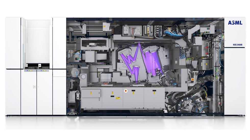
This photo-illustration of the EXE:5000, ASML’s high-numerical-aperture extreme-ultraviolet-lithography machine, shows its massive scale.
Source: ASML
DarkBlue2
Over the last half-century, we’ve come to think of Moore’s Law—the roughly biennial doubling of the number of transistors in a given area of silicon, the gains that drive computing forward—as something that just happens, as though it were a natural, inevitable process, akin to evolution or aging. The reality, of course, is much different. Keeping pace with Moore’s Law requires almost unimaginable expenditures of time, energy, and human ingenuity—thousands of people on multiple continents and endless acres of some of the most complex machinery on the planet.
Perhaps the most essential of these machines performs extreme-ultraviolet (EUV) photolithography. EUV lithography, the product of decades of R&D, is now the driving technology behind the past two generations of cutting-edge chips, used in every top-end smartphone, tablet, laptop, and server in the last three years. Yet Moore’s Law must march on, and chipmakers continue to advance their road maps, meaning they’ll need to shrink device geometries even further.
So at ASML, my colleagues and I are developing the next generation of lithography. Called high-numerical-aperture EUV lithography, it involves a major overhaul of the system’s internal optics. High-NA EUV should be ready for commercial use in 2025, and chipmakers are depending on its capabilities to keep their promised advances through the end of this decade
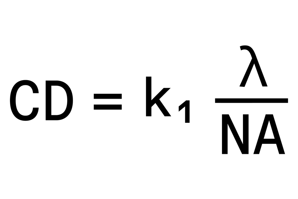
The 3 factors of photolithography
Moore’s Law relies on improving the resolution of photolithography so chipmakers can lay down finer and finer circuits. Over the last 35 years, engineers have achieved a resolution reduction of two orders of magnitude by working on a combination of three factors: the wavelength of the light; k 1, a coefficient that encapsulates process-related factors; and numerical aperture (NA), a measure of the range of angles over which the system can emit light.
 Source: IEEE Spectrum
The critical dimension—that is, the smallest possible feature size you can print with a certain photolithography-exposure tool—is proportional to the wavelength of light divided by the numerical aperture of the optics. So you can achieve smaller critical dimensions by using either shorter light wavelengths or larger numerical apertures or a combination of the two. The k 1 value can be pushed as close as possible to its physical lower limit of 0.25 by improving manufacturing-process control, for example.
In general, the most economical ways to boost resolution are by increasing the numerical aperture and by improving tool and process control to allow for a smaller k 1. Only after chipmakers run out of options to further improve NA and k1 do they resort to reducing the wavelength of the light source.
Nevertheless, the industry has had to make that wavelength change a number of times. The historical progression of wavelengths went from 365 nanometers, generated using a mercury lamp, to 248 nm, via a krypton-fluoride laser, in the late 1990s, and then to 193 nm, from an argon-fluoride laser, at the beginning of this century. For each generation of wavelength, the numerical aperture of lithography systems was progressively increased before industry jumped to a shorter wavelength.
For example, as the use of 193 nm was coming to an end, a novel approach to increasing NA was introduced: immersion lithography. By placing water between the bottom of the lens and the wafer, the NA could be significantly enlarged from 0.93 to 1.35. From its introduction around 2006, 193-nm immersion lithography was the industry workhorse for leading-edge lithography
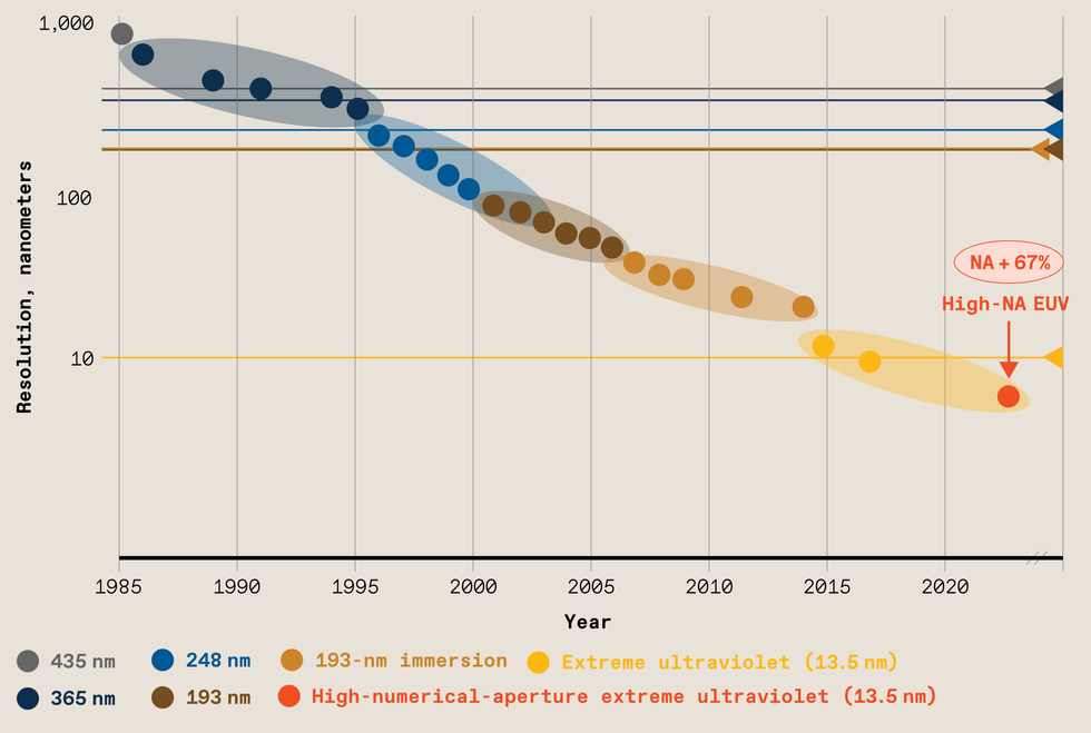 The resolution of photolithography has improved by about two order os magnitude over the last 35 years. That’s due in part to using smaller and smaller wavelengths of light, but it has also required greater numerical aperture and improved processing techniques.Source: ASML
The dawn of EUV
But as the need to print features smaller than 30 nm increased, and because the NA of 193-nm lithography had been maxed out, keeping up with Moore’s Law grew more and more complex. To create features smaller than 30 nm requires either using multiple patterns to produce a single layer of chip features—a technologically and economically burdensome technique—or another change of wavelength. It took more than 20 years and an unparalleled development effort to bring the next new wavelength online: 13.5-nm EUV.
EUV necessitates an entirely new way to generate light. It’s a remarkably complex process that involves hitting molten tin droplets in midflight with a powerful CO2 laser. The laser vaporizes the tin into a plasma, emitting a spectrum of photonic energy. From this spectrum, the EUV optics harvest the required 13.5-nm wavelength and direct it through a series of mirrors before it is reflected off a patterned mask to project that pattern onto the wafer. And all of this must be done in an ultraclean vacuum, because the 13.5-nm wavelength is absorbed by air. (In previous generations of photolithography, light was directed through the mask to project a pattern onto the wafer. But EUV is so readily absorbed that the mask and other optics must be reflective instead.)
 In a vacuum chamber, EUV light [purple] reflects off multiple mirrors before bouncing off the photomask [top center]. From there the light continues its journey until it is projected onto the wafer [bottom center], carrying the photomask’s pattern. The illustration shows today’s commercial system with a 0.33 numerical aperture. The optics in future systems, with an NA of 0.55, will be different.Source: ASML
The switch to EUV from 193-nanometer light did part of the job of decreasing the critical dimension. A process called “design for manufacturing,” which involves setting the design rules of circuit blocks to take advantage of photolithography’s limits, has done a lot to reduce k
1. Now it’s time to boost numerical aperture again, from today’s 0.33 to 0.55.
Making high-NA EUV work
Increasing the NA from today’s 0.33 to the target value of 0.55 inevitably entails a cascade of other adjustments. Projection systems like EUV lithography have an NA at the wafer and also at the mask. When you increase the NA at the wafer, it also increases the NA at the mask. Consequently, at the mask, the incoming and outgoing cones of light become larger and must be angled away from each other to avoid overlapping. Overlapping cones of light produce an asymmetric diffraction pattern, resulting in unpleasant imaging effects.
But there’s a limit to this angle. Because the reflective masks needed for EUV lithography are actually made of multiple layers of material, you can’t ensure getting a proper reflection above a certain reflective angle. EUV masks have a maximum reflective angle of 11 degrees. There are other challenges as well, but reflective angle is the biggest.
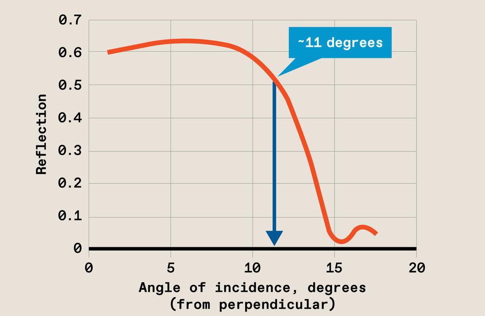 If the EUV light strikes the photomask at too steep an angle, it will not reflect properly.Source: ASML
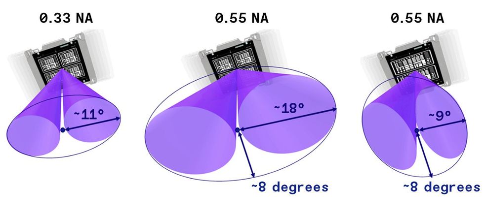 The angle of reflection at the mask in today’s EUV is at its limit [left] Increasing the numerical aperture of EUV would result in an angle of reflection that is too wide [center]. So high-NA EUV uses anamorphic optics, which allow the angle to increase in only one direction [right]. The field that can be imaged this way is half the size, so the pattern on the mask must be distorted in one direction, but that’s good enough to maintain throughput through the machine.Source: ASML
The only way to overcome this challenge is to increase a quality called demagnification. Demagnification is exactly what it sounds like—taking the reflected pattern from the mask and shrinking it. To compensate for the reflective-angle problem, my colleagues and I had to double the demagnification to 8x. As a consequence, the part of the mask imaged will be much smaller on the wafer. This smaller image field means it will take longer to produce the complete chip pattern. Indeed, this requirement would reduce the throughput of our high-NA scanner to under 100 wafers per hour—a productivity level that would make chip manufacturing uneconomical.
Thankfully, we found that it is necessary to increase the demagnification in only one direction—the one in which the largest reflective angles occur. The demagnification in the other direction can remain unchanged. This results in an acceptable field size on the wafer—about half the size used in today’s EUV systems, or 26 by 16.5 millimeters instead of 26 by 33 mm. This kind of direction-dependent, or anamorphic, demagnification forms the basis of our high-NA system. The optics manufacturer Carl Zeiss has made a herculean effort to design and manufacture an anamorphic lens with the specifications required for our new machine.
To ensure the same productivity levels with the half-size field, we had to redevelop the system’s reticle and wafer stages—the platforms that hold the mask and wafer, respectively, and move them in sync with each other as the scanning process takes place. The redesign resulted in nanometer-precision stages with acceleration improved by a factor of four.
High-NA EUV in production in 2025
The first high-NA EUV system, the ASML EXE:5000, will be installed in a new lab that we’re opening jointly with the Belgium-based nanoelectronics research facility Imec, in early 2024. This lab will allow customers, mask makers, photoresist suppliers, and others to develop the infrastructure needed to make high-NA EUV a reality.
And it is essential that we do make it a reality, because high-NA EUV is a critical component in keeping Moore’s Law alive. Getting to 0.55 NA won’t be the final step, though. From there, ASML, Zeiss, and the entire semiconductor ecosystem will be stretching even further toward technologies that are better, faster, and innovative in ways we can hardly imagine yet.
This article appears in the September 2023 print issue as “The Moore’s Law Machine.”
From Your Site Articles
- The Semiconductor Industry’s Most Important Tool Goes Green ›
- EUV Lithography Finally Ready for Chip Manufacturing ›
- None ›
- Canon Delivers Nanoimprint Lithography to Compete With EUV - IEEE Spectrum ›
Related Articles Around the Web
{"imageShortcodeIds":[]}


