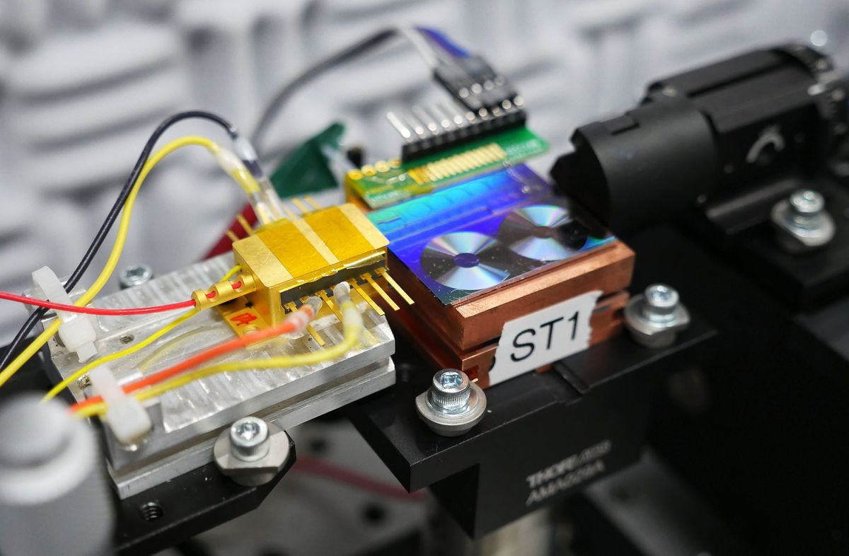
Exquisite timing is essential to many important technologies, including GPS navigation and radar. Optical approaches provide the most precise and stable timing signals, but they require bulky equipment that makes them impractical in many situations. Now, researchers at the National Institute of Standards and Technology (NIST) have created an optical timing system small enough to fit on a single chip, greatly expanding where the technology could be used.
Even the most sophisticated clocks are susceptible to tiny errors, a phenomenon know as timing jitter. Minimizing jitter is crucial for the wide range of technologies that rely on precise timekeeping. In GPS navigation, your location is determined by measuring how long it takes for time-stamped signals from multiple satellites to reach your receiver. Errors in the timestamps can quickly add up to sizeable positioning errors. Similarly, any fuzziness in the time signals used to coordinate large numbers of simultaneous data streams on a telecoms network can lead to delays or dropped calls. And radar relies on being able to accurately time how long it takes for electromagnetic signals to bounce back off targets like air planes and rain clouds.
The resulting oscillator has reduced the jitter in the system to just 15 femtoseconds
Today, these applications rely on microwave oscillators. While a traditional clock might use a pendulum swinging back and forth to measure the passage of time, microwave oscillator clocks rely on electric fields that fluctuate at frequencies of 300 MHz to 300 GHz. Such rapid fluctuations mean you can divide time up much more precisely, says Frank Quinlan, NIST physical scientist, because the signal “ticks” many more times in a given period.
But optical signals have long been recognised as a promising alternative, because they oscillate even faster, at hundreds of terahertz. The problem is that these frequencies are simply too high for electronic circuits to interface with directly, and the complex set ups required to convert an optical signal into an electronic one are relatively bulky and complex.
Now, a multi-institution team led by NIST has succeeded in creating an optical timing system out of chip-sized components. The resulting oscillator has reduced the jitter in the system to just 15 femtoseconds (a femtosecond is a quadrillionth of a second), orders of magnitude better than traditional microwave-based systems.
“The precision and timing that you can get with optical signals, you just cannot get with standard microwave electronics,” says Qunilan, who led the research. “This is taking those tabletop, lab-scale experiments and shrinking them down to the chip-scale.”
Getting to this point was a long road, says Quinlan. The research builds on decades of progress in silicon photonics, in particular efforts to shrink a critical component known as a frequency comb down to chip-scale. Optical frequency combs are lasers that generate light in a wide range of frequencies, but only at sharply defined frequencies, so the spectrum has a set of peaks that are evenly spaced like the teeth of a comb, hence the name. They can also be used to measure and convert signals between frequencies, which is why they are often referred to as “rulers for light”.
“This work shows a path towards truly chip-scale devices.”
“Getting optical frequency combs from tabletop experiments to chip-scale has been a long effort in the community,” says Qunlan. “So that is an enabling technology for what we’ve done here.”
The new device features a pair of ultra-low noise semiconductor lasers that are fired into a reflective optical cavity. As the laser light bounces around inside, frequencies matched to the size of the cavity build up in power creating a highly stable light source. This is then passed to a frequency comb, which downtunes the light signal to microwave frequencies. That signal is then passed to a photodetector that translates it into an electronic one that can interface with other devices. The researchers describe the set up in a paper in Nature.
“It is a very nice accomplishment,” says Tobias Kippenberg, professor of physics the Swiss Federal Institute of Technology Lausanne, who led the lab at the Max Planck Institute of Quantum Optics in Garching, Germany, that first developed tiny optical frequency combs known as “microcombs”. “This work shows a path towards truly chip-scale devices.”
The stabilizing cavity the researchers use is probably not necessary, he says, and could probably be done away with by altering the design of the frequency comb. But the demonstration is nonetheless impressive, he adds, and shows a clear path towards commercial deployment.
That will still require some work though, says Quinlan. While all the components used are chip-scale, the team deliberately spread them over several chips so they could independently measure their performance and better understand their underlying physics. This helped them better understand the footprint each requires, as well as their power needs and heat generation.
This will help inform the process of integrating them all on a single chip, says Quinlan, which is now the team’s main focus. He says there are no fundamental physical barriers and it’s mainly a matter of engineering, but creating a device ready for the real world will take time.
“It’s going to be a lot of work on environmental testing, to make it really feasible to get out of the lab,” he says. “We’re going to learn a lot when we cycle the temperature and when we put it on vibration platforms.”
Edd Gent is a freelance science and technology writer based in Bengaluru, India. His writing focuses on emerging technologies across computing, engineering, energy and bioscience. He's on Twitter at @EddytheGent and email at edd dot gent at outlook dot com. His PGP fingerprint is ABB8 6BB3 3E69 C4A7 EC91 611B 5C12 193D 5DFC C01B. His public key is here. DM for Signal info.


