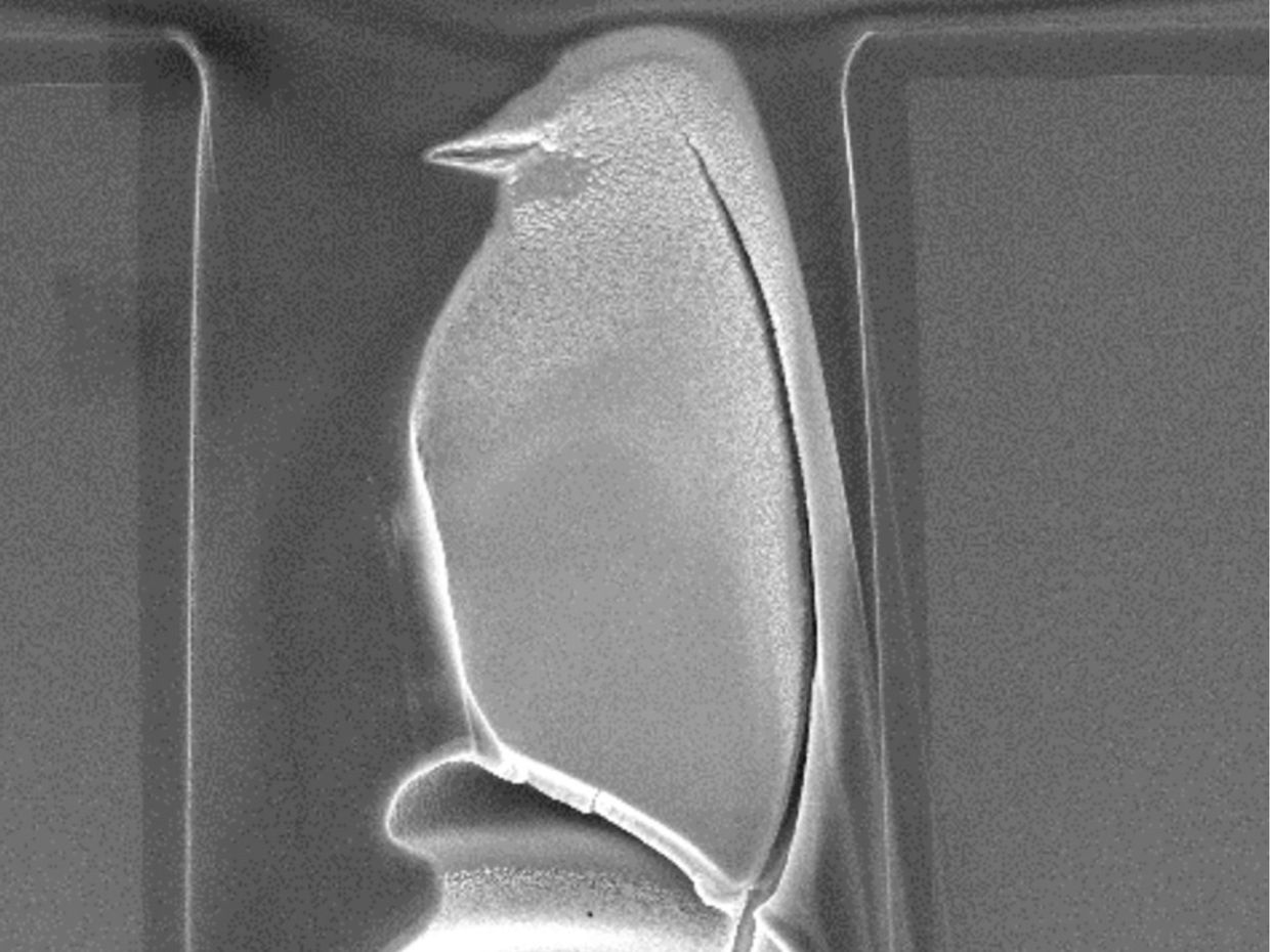
Photo: Lew Li Lian/GlobalFoundriesBirdie in the Hole: This little bird sits contentedly under the microscope’s gaze, but it didn’t fly there on its own. According to Lew Li Lian from GlobalFoundries, in Singapore, “A particle in the hole caused a cavity formation in the precoat material, resembling a birdie.” It won first prize at the 2014 IEEE International Symposium on the Physical and Failure Analysis of Integrated Circuits (IPFA) Art of Failure Analysis contest. ▲
Photo: Khoo Bingsheng/WinTech Nano-Technology Services Hibiscus: Khoo Bingsheng from WinTech Nano-Technology Services, in Singapore, was shocked to see flowers in bloom on the top layer of his gallium nitride sample. He took a series of zoom images until he found a perfect depiction and hopes the image will “bring happiness to all.” ▲
Photo: Muhamad Hilmi/ON SemiconductorLovebirds: A surface analysis of metal with a peeling problem revealed these birds on a branch. Muhamad Hilmi Rosnan from On Semiconductor, in Malaysia, thought nothing of the picture when he first captured it, but when he heard about the contest, he looked back through his trove of images and found “loving birds on a tree branch.” ▲
Photo: Lee Nean Sern/InfineonHand Holding a Lemon: Lee Nean Sern of Infineon Technologies, in Malaysia, was testing a transistor experiencing early failure when he ran into what looked like fingers clutching a lemon’s cross section. As it turned out, improper etching had caused a short and inscribed this scene onto the metal. ▲
Photo: Leonardo Vinalon/Analog DevicesSea Horse: Leonardo Vinalon from Analog Devices, in the Philippines, identified this little creature relaxing on the surface of a glass seal. ▲
Photo: Lim Wei Chuan/Infineon TechnologiesEye With Tear: When Lim Wei Chuan from Infineon Technologies, in Malaysia, inspected this irregularity, he discovered a tearful eye there to greet him. An uneven layer of underlying metal beneath led to this sad expression. ▲
Photo: Rudolf A. Sia/Analog DevicesGrand Canyon: This vivid landscape is actually the fracture surface of a silicon die, according to Rudolf A. Sia from Analog Devices, in the Philippines. ▲
Photo: Phang Nyuk Lin/GlobalFoundriesNuptial Snails: After a sample was etched, Phang Nyuk Lin of GlobalFoundries, in Singapore, discovered that these snails—apparently in brides’ veils—had crawled onto the scene. ▲
Photo: Lim Chan Way/Infineon TechnologiesSculpture of a Monk: Lim Chan Way from Infineon Technologies, in Malaysia, discovered this “bald-headed man with plain appearance” when cleaving a sample. The industrious monk could have emerged from a light-sensitive material or silicon residue. ▲
Photo: Chng Kheaw Chung/Systems on Silicon Manufacturing Co.White Christmas: This delicate snowflake has arms just 20 micrometers long. Chng Kheaw Chung of Systems on Silicon Manufacturing Co., in Singapore, captured the image of crystallization after cleaning a sample. ▲
IEEE Spectrum is the flagship publication of the IEEE — the world’s largest professional organization devoted to engineering and applied sciences. Our articles, podcasts, and infographics inform our readers about developments in technology, engineering, and science.
IEEE Spectrum is the flagship publication of the IEEE — the world’s largest professional organization devoted to engineering and applied sciences. Our articles, podcasts, and infographics inform our readers about developments in technology, engineering, and science.