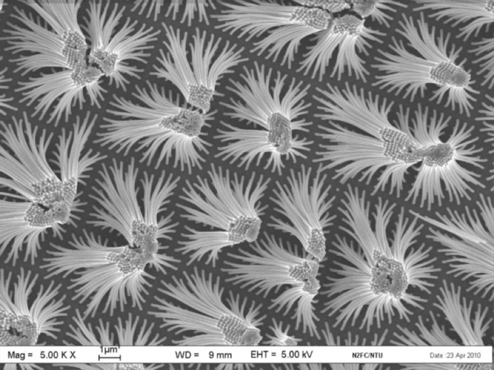
Image: Rahmat Agung SusantyokoThis year’s first-prize winner in the “Art of Failure Analysis” contest is an image of a bed of 0.13-micrometer-wide “nanoflowers” sitting on a silicon substrate. The flowers “blossomed” when an array of vertically oriented silicon nanowires bent from their original upright position. Rahmat Agung Susantyoko, who took the image, was given the task of monitoring the height of arrays of silicon nanowires. Nanowires of a certain height bent together to form the flowers. ▲
Image: Tang Lei JunA city built entirely of gallium nitride? This Atlantis was uncovered with a focused ion beam technique, which uses a ray of ions to etch, polish, and deposit material on a sample. It won second prize. < ▲
Image: Ng Boon Haur & Oh Siew KhimA particle that fell onto a wafer formed this creature, which analysts at Systems on Silicon Manufacturing, in Singapore, thought looked like a worker ant carrying away a defect. ▲
Image: Foo Fang JieThis stoic-looking robot was spied while engineers were preparing a die for transmission electron microscopy. The face appeared as the copper metal layers were being thinned using a focused ion beam machine. ▲
Image: Jacqueline KwaSometimes technology mimics nature. A copper grid and the platinum metal deposited on it were ejected at different rates by a beam of energetic ions, and the result was a platinum lily in a copper valley. ▲
Image: Joey PhuaSolder bumps, when melted, join chips to external circuits. During the deconstruction of one such arrangement, analysts at Advanced Micro Devices shuddered at the sight of this image, which looked to them like a brain infested with maggots. ▲
Image: Ng Lay SimWhat analysts visualize during failure analysis sometimes has more to do with the chores on their to-do lists than the task at hand. This submission shows a silicon sample being thinned for transmission electron microscopy. The area on the right side of the image cut more slowly than the rest of the layer, resulting in a clothespin-like shape that reminded the analyst to do his laundry. < ▲
Image: Re-Long Chiu & Tim SchnutenhausYou can’t help but smile back at this beaming “face,” which is actually a defective memory cell stained with a chemical solution. Analysts snapped this cheerful image while investigating the cause of the device’s low breakdown voltage. ▲
Image: Ho Mun YeeThose who discovered this image likened it to a bird’s-eye view of an expansive metropolis, but it actually shows copper metal “rising up” from a silicon oxide base. Analysts etched away at the silicon oxide with a focused beam of ionic gas while the copper remained intact. ▲
Image: Seah Pei HongDon’t pucker up for these lips. They’re actually a tungsten crater in an IC. The suggestive image was captured using transmission electron microscopy. ▲
IEEE Spectrum is the flagship publication of the IEEE — the world’s largest professional organization devoted to engineering and applied sciences. Our articles, podcasts, and infographics inform our readers about developments in technology, engineering, and science.
IEEE Spectrum is the flagship publication of the IEEE — the world’s largest professional organization devoted to engineering and applied sciences. Our articles, podcasts, and infographics inform our readers about developments in technology, engineering, and science.