The fine art of adding impurities to silicon wafers lies at the heart of semiconductor engineering and, with it, much of the computer industry. But this fine art isn’t yet so finely tuned that engineers can manipulate impurities down to the level of individual atoms.
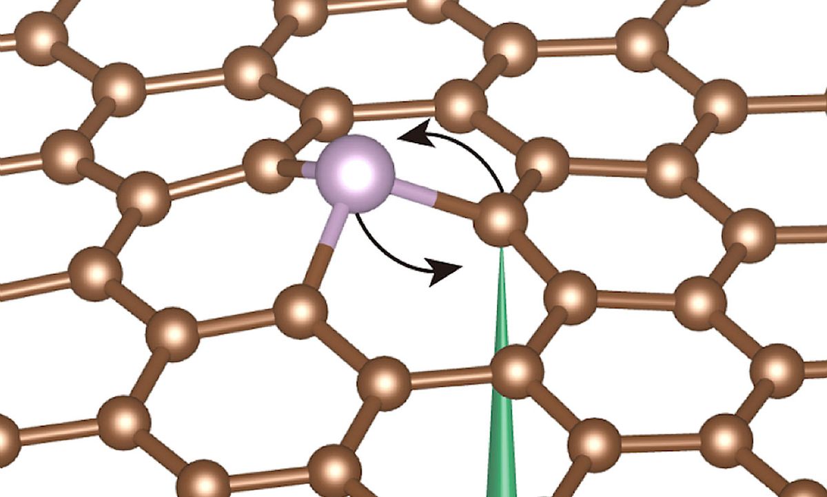
As technology scales down to the nanometer size and smaller, though, the placement of individual impurities will become increasingly significant. Which makes interesting the announcement last month that scientists can now rearrange individual impurities (in this case, single phosphorous atoms) in a sheet of graphene by using electron beams to knock them around like croquet balls on a field of grass.
The finding suggests a new vanguard of single-atom electronic engineering. Says research team member Ju Li, professor of nuclear science and engineering at MIT, gone are the days when individual atoms can only be moved around mechanically—often clumsily on the tip of a scanning tunneling microscope.
Instead, using the electron beam of a scanning transmission electron microscope (STEM), the same device that can image an atomic landscape can now also be used to push individual atoms across that landscape. And because the beam is steered by magnetic fields, it can perform its operations in small fractions of the time it would take to mechanically maneuver the tip of a tunneling microscope from place to place. (Li says his group’s new technology could in fact move atoms around in the span of microseconds.)
On top of that, Li says, nothing would prevent the new technology from being rolled out with many electron beams operating at once—with possibly smart algorithms, not human operators, steering the beams. Which could mean these single-atom electronic engineering techniques might be able to scale up to technologically useful levels, and not just be limited to one-shot, lab bench curios.
“We can create a defect at the location that we want with absolute certainty where each atom sits,” Li says. “So that is a completely different regime of engineering.”
In the case of the present research, then, a graphene sheet with pre-existing dopant phosphorous atoms sprinkled throughout its lattice are put into the STEM. The electron microscope images the mostly carbon sheet and locates the spots where phosphorous impurities lie. Researchers then used the electron beam to move those phosphorous atoms around.
Li says the new work presents several novel innovations. The first is the simple ability to move individual atoms around so rapidly and the potential to scale up this technique. Underlying its scalability, then, is their other chief innovation: A theory that describes how and where to point an electron beam so that an atomic impurity is nudged through a graphene lattice to its ultimate destination.
The scheme, what the researchers call “primary knock-on space” (PKS) theory, is like the ultimate catalog of billiards trick shots. Come at atom X with such-and-such an angle and energy, and you’ll find it swaps places with the next carbon atom down the line. And so on.
So their PKS theory provides the mathematical guts to any smart algorithm that might one day automatically move phosphorous (or other impurities) around a 2D lattice.
In fact, Li says, PKS theory now appears applicable to other impurities in other 2D atomic sheets. One planar material that shows promise like graphene (and that Spectrum has previously covered) is so-called hexagonal boron nitride.
Impurities in h-BN are currently attractive candidates for quantum sensors and quantum computing chips. Earlier this year, Spectrum profiled a research effort to develop qubits around impurities wherever-they-may-lie on an h-BN sheet. Li says his group is now working to move those impurities in h-BN around so they’re not in random placements but rather in a predetermined set of locations.
“There is an ecosystem there,” says Li of the quantum technologies being developed for h-BN today. “It’s like a chicken and egg situation. People say it would be nice if we had this kind of defect [in h-BN], but they don’t know how to create it. And we can create a whole bunch of defects, but we don’t know what kind of quantum [technologies] we can do.”
Margo Anderson is senior associate editor and telecommunications editor at IEEE Spectrum. She has a bachelor’s degree in physics and a master’s degree in astrophysics.


