A new kind of transistor consumes 90 percent less power than conventional transistors, dramatically exceeding a theoretical limit for electronics, researchers say. These findings could one day lead to super-dense low-power circuits as well as ultra-sensitive biosensors and gas sensors, the investigators added.
The relentless advance of computing power over the past half-century has relied on constant miniaturization of field-effect transistors (FETs), which serve as the building blocks of most microchips. Transistors act like switches that flick on and off to represent data as zeroes and ones.
A key challenge that FETs now face is reducing the power they consume. The switching properties of conventional FETs are currently restricted by a theoretical limit of 60 millivolts per decade of current at room temperature. This limit, known as the subthreshold swing, means that each 60-millivolt increase in voltage leads to a 10-fold increase in current. Lowering the swing would yield better channel control, so switching would require less energy.
One way that scientists have sought to overcome this limit is with tunnel FETs (TFETs). These devices take advantage of the ability of electrons to penetrate barriers, a phenomenon known as quantum tunneling. In theory, quantum tunneling should enable TFETs to switch on and off with much lower voltages than conventional FETs.
Now researchers at the University of California, Santa Barbara (UCSB), and Rice University in Houston, Texas, have developed a TFET that could operate with voltages as low as 0.1 volts. This led to a more than 90 percent reduction in power consumption compared with conventional FETs. The scientists and engineers detailed their findings in the 1 Oct. issue of the journal Nature.
“This transistor represents a major breakthrough in the electronics and semiconductor industry,” says study co-author Kaustav Banerjee, an electrical engineer at UCSB.
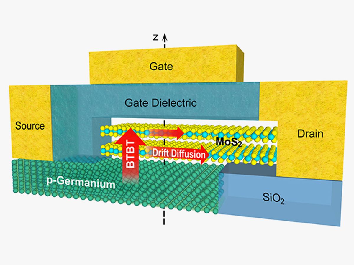
The new TFET is made from two atomically-thin layers of semiconducting molybdenum sulfide crystal on top of a substrate of germanium. It achieved a subthreshold swing as little as 3.9 millivolts per decade of current.
Until now, the only experimental TFET to meet the International Technology Roadmap for Semiconductors’ (ITRS’s) goal of average subthreshold swing below 60 millivolts per decade over four decades of current was a transistor that used nanowires. But that type is often challenging to fabricate using conventional semiconductor manufacturing techniques. This new TFET not only meets the ITRS goal, it also uses flat channels that are easier to fabricate.
UCSB’s Banerjee suggests that potential applications for these new TFETs may include ultra-low-power electronics and computing, longer battery life or lower power consumption in data centers to reduce their costs and greenhouse gas emissions, and ultra-sensitive and low-power biosensors and gas sensors to enhance the Internet of Things.
However, Banerjee cautions that TFETs are not designed for speed or high performance. “They are desirable for low-power electronics,” he says.
Charles Q. Choi is a science reporter who contributes regularly to IEEE Spectrum. He has written for Scientific American, The New York Times, Wired, and Science, among others.


