
 Illustration: Serge Bloch

A half century ago, a young engineer named Gordon E. Moore took a look at his fledgling industry and predicted big things to come in the decade ahead. In a four-page article in the trade magazine Electronics, he foresaw a future with home computers, mobile phones, and automatic control systems for cars. All these wonders, he wrote, would be driven by a steady doubling, year after year, in the number of circuit components that could be economically packed on an integrated chip.
A decade later, the exponential progress of the integrated circuit—later dubbed “Moore’s Law”—showed no signs of stopping. And today it describes a remarkable, 50-year-long winning streak that has given us countless forms of computers, personal electronics, and sensors. The impact of Moore’s Law on modern life can’t be overstated. We can’t take a plane ride, make a call, or even turn on our dishwashers without encountering its effects. Without it, we would not have found the Higgs boson or created the Internet.
But what exactly is Moore’s Law, and why has it been so successful? Is it evidence of technology’s inevitable and unstoppable march? Or does it simply reflect a unique time in engineering history, when the special properties of silicon and a steady series of engineering innovations conspired to give us a few decades of staggering computational progress?
I would argue that nothing about Moore’s Law was inevitable. Instead, it’s a testament to hard work, human ingenuity, and the incentives of a free market. Moore’s prediction may have started out as a fairly simple observation of a young industry. But over time it became an expectation and self-fulfilling prophecy—an ongoing act of creation by engineers and companies that saw the benefits of Moore’s Law and did their best to keep it going, or else risk falling behind the competition.
I would also argue that, despite endless paraphrasing, Moore’s Law is not one simple concept. Its meaning has changed repeatedly over the years, and it’s changing even now. If we’re going to draw any lessons from Moore’s Law about the nature of progress and what it can tell us about the future, we have to take a deeper look.
In the early 1960s, before Silicon Valley became known as Silicon Valley, Gordon Moore was director of research and development at Fairchild Semiconductor. He and others had founded the company in 1957 after defecting from Shockley Semiconductor Laboratory, where they’d done some of the early work on silicon electronic devices.
Fairchild was one of a small group of companies working on transistors, the now ubiquitous switches that are built by the billions onto chips and are used to perform computations and store data. And the firm quickly started carving out a niche.
At the time, most circuits were constructed from individual transistors, resistors, capacitors, and diodes that were wired together by hand on a circuit board. But in 1959, Jean Hoerni of Fairchild invented the planar transistor—a form of transistor that was constructed in the plane of the silicon wafer instead of on a raised plateau, or mesa, of silicon.
With this configuration, engineers could build wires above the transistors to connect them and so make an “integrated circuit” in one fell swoop on the same chip. Jack Kilby of Texas Instruments had pioneered an early integration scheme that connected devices with “flying wires” that rose above the surface of the chip. But Moore’s colleague Robert Noyce showed that planar transistors could be used to make an integrated circuit as a solid block, by coating the transistors with an insulating layer of oxide and then adding aluminum to connect the devices. Fairchild used this new architecture to build the first silicon integrated circuit, which was announced in 1961 and contained a whopping four transistors. By 1965, the company was getting ready to release a chip with roughly 64 components.
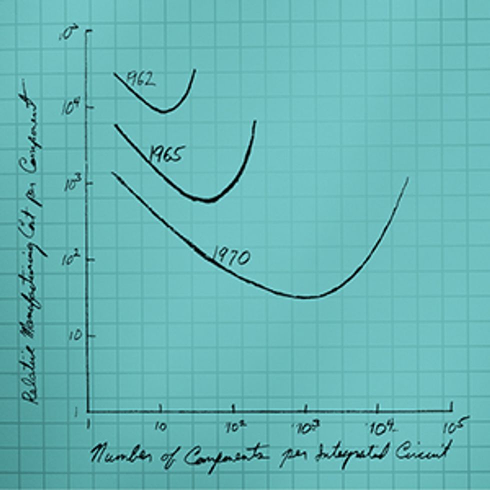 The Sweet Spot: Economics was at the core of Moore’s 1965 paper. He argued that for any particular generation of manufacturing technology, there is a cost curve. The cost of making a component declines the more you pack onto an integrated circuit, but past a certain point, yields decline and costs rise. The sweet spot, where the cost per component is at a minimum, moves to more and more complex integrated circuits over time.Image: Intel
Armed with this knowledge, Moore opened his 1965 paper with a bold statement: “The future of integrated electronics is the future of electronics itself.” That claim seems self-evident today, but at the time it was controversial. Many people doubted that the integrated circuit would ever fill anything more than a niche role.
You can forgive the skepticism. Although the first integrated chips were more compact than their hand-wired brethren, they cost significantly more. Only a handful of companies were making integrated circuits, and their only real customers were NASA and the U.S. military.
Compounding the problem was the fact that transistors were still unreliable. Of the individual transistors that were made, only a small fraction—just 10 to 20 percent, Moore later recalled—actually worked. Pack a half dozen of those devices together in an integrated circuit and you’d expect those small fractions to multiply, yielding a dismally small number of operational chips.
But this logic was flawed. It turned out that making a chip with eight transistors yields a fraction of operational chips similar to what you’d get by making eight stand-alone transistors. That’s because the probabilities aren’t independent. Defects take up space, and many types are distributed randomly, like paint splatter. If two transistors are placed close together, a single transistor-size flaw can take out both devices. As a result, putting two transistors side by side carries about the same risk of death by defect as one transistor by itself.
Moore was convinced that integration would ultimately prove economical. In his 1965 paper, as evidence of the integrated circuit’s bright future, he plotted five points over time, beginning with Fairchild’s first planar transistor and followed by a series of the company’s integrated circuit offerings. He used a semilogarithmic plot, in which one axis is logarithmic and the other linear and an exponential function will appear as a straight line. The line he drew through the points was indeed more or less straight, with a slope that corresponded to a doubling of the number of components on an integrated circuit every year.
From this small trend line, he made a daring extrapolation: This doubling would continue for 10 years. By 1975, he predicted, we’d see the number of components on an integrated circuit go from about 64 to 65,000. He got it very nearly right. By 1975, Intel, the company Moore cofounded after leaving Fairchild in 1968, was preparing charged-coupled-device (CCD) memory chips with some 32,000 components—only a factor of two off from his thousandfold prediction.
Looking back on this remarkable paper, I’ll note a few details that are often overlooked. First, Moore’s prediction was about the number of electronic components—not just transistors but also devices such as resistors, capacitors, and diodes. Many early integrated circuits actually had more resistors than transistors. Later, metal-oxide-semiconductor (MOS) circuitry, which relied less on nontransistor components, emerged, and the digital age began. Transistors dominated, and their number became the more useful measure of integrated circuit complexity.
The paper also reveals Moore’s focus on the economics of integration. He defined the number of components per chip not as the maximum or the average number of components but as the number for which the cost per component was at a minimum. He understood that the number of components that you can pack on a chip and the number that makes economic sense are not necessarily the same. Instead, there’s a sweet spot for every generation of chip-fabrication technology. As you add more components, you drive the cost per component down. But past a certain point, attempting to pack even more transistors into a given space will raise the possibility of killer defects and lower the yield of useful chips. At that point, the cost per component will start to rise. The goal of integrated circuit design and manufacturing was—and still is—to hit this sweet spot.
As chip-fabrication technology has improved, the sweet spot has shifted to larger numbers of components and lower costs per component. Over the last 50 years, the cost of an integrated circuit transistor has been reduced from $30 in today’s dollars to a nanodollar or so. Moore could hardly have predicted such a dramatic reduction. But even in 1965, he understood that integrated circuits were about to change from an expensive, high-performance replacement for discrete components to a cheap, high-performance replacement, and that both performance and economics would favor integration.
Ten years later, Moore revisited his prediction and revised it. In an analysis he’d done for the 1975 IEEE International Electron Devices Meeting, he started by tackling the question of how the doubling of components actually happened. He argued that three factors contributed to the trend: decreasing component size, increasing chip area, and “device cleverness,” which referred to how much engineers could reduce the unused area between transistors.
Moore attributed about half of the doubling trend to the first two factors and the rest to “cleverness.” But when he considered the CCD memories that Intel was preparing to release, he decided that cleverness would soon go out the window. In CCD arrays, devices are packed together in tight grids with no wasted space to eliminate. So he predicted the doubling trend would soon be driven only by tinier transistors and bigger chips. As a result it would slow by half, doubling components once every two years instead of every year.
Ironically, CCD memory proved to be too error prone, so Intel stopped pursuing it. But the prediction was nonetheless borne out in logic chips, such as microprocessors, which have grown at about a two-year doubling rate since the early 1970s. Memory chips, with their massive arrays of identical transistors, scaled faster, doubling every 18 months or so, mainly because they are simpler to design.
Of the three technology drivers Moore identified, one turned out to be special: decreasing the dimensions of the transistor. For a while at least, shrinking transistors offered something that rarely happens in the world of engineering: no trade-offs. Thanks to a scaling rule named for IBM engineer Robert Dennard, every successive transistor generation was better than the last. A shrinking transistor not only allowed more components to be crammed onto an integrated circuit but also made those transistors faster and less power hungry.
This single factor has been responsible for much of the staying power of Moore’s Law, and it’s lasted through two very different incarnations. In the early days, a phase I call Moore’s Law 1.0, progress came by “scaling up”—adding more components to a chip. At first, the goal was simply to gobble up the discrete components of existing applications and put them in one reliable and inexpensive package. As a result, chips got bigger and more complex. The microprocessor, which emerged in the early 1970s, exemplifies this phase.
But over the last few decades, progress in the semiconductor industry became dominated by Moore’s Law 2.0. This era is all about “scaling down,” driving down the size and cost of transistors even if the number of transistors per chip does not go up.
Although the Moore’s Law 1.0 and 2.0 eras have overlapped, the dominance of scaling down versus scaling up can be seen in the way the semiconductor industry describes itself. In the 1980s and early 1990s, the technology generations, or “nodes,” that define progress in the industry were named after dynamic RAM generations: In 1989, for example, we had the 4-megabyte DRAM node; in 1992, the 16-MB node. Each generation meant greater capability within a single chip as more and more transistors were added without raising the cost.
By the early 1990s, we’d begun to name our nodes after the shrinking features used to make the transistors. This was only natural. Most chips didn’t need to carry as many transistors as possible. Integrated circuits were proliferating, finding their way into cars and appliances and toys, and as they did so, the size of the transistor—with the implications for performance and cost savings—became the more meaningful measure.
Eventually even microprocessors stopped scaling up as fast as manufacturing technology would permit. Manufacturing now allows us to economically place more than 10 billion transistors on a logic chip. But only a few of today’s chips come anywhere close to that total, in large part because our chip designs generally haven’t been able to keep up.
Moore’s Law 1.0 is still alive today in the highest-end graphics processing units, field-programmable gate arrays, and perhaps a handful of the microprocessors aimed at supercomputers. But for everything else, Moore’s Law 2.0 dominates. And now it’s in the process of changing again.
This change is happening because the benefits of miniaturization are progressively falling away. It began in the early 2000s, when an unpleasant reality started to emerge. At that time, transistor sizes began to creep down below 100 nanometers, and Dennard’s simple scaling rule hit its limit. Transistors became so small that it was quite easy for electrons to sneak through them even when the devices were supposed to be off, leaking energy and lowering device reliability. Although new materials and manufacturing techniques helped combat this problem, engineers had to stop the practice of dramatically lowering the voltage supplied to each transistor in order to maintain a strong electrical clamp.
Because of the breakdown of Dennard scaling, miniaturization is now full of trade-offs. Making a transistor smaller no longer makes it both faster and more efficient. In fact, it’s very difficult to shrink today’s transistors and maintain even the same speed and power consumption of the previous generation.
As a result, for the last decade or so, Moore’s Law has been more about cost than performance; we make transistors smaller in order to make them cheaper. That isn’t to say that today’s microprocessors are no better than those of 5 or 10 years ago. There have been design improvements. But much of the performance gains have come from the integration of multiple cores enabled by cheaper transistors.
The economics has remained compelling because of an important and unheralded feature of Moore’s Law: As transistors have gotten smaller, we’ve been able to keep the cost of manufacturing each square centimeter of finished silicon about the same, year after year after year (at least until recently). Moore has put it at about a billion dollars an acre—although chipmakers seldom think in terms of acreage.
Keeping the cost of finished silicon constant for decades hasn’t been easy. There was steady work to improve yield, which started in the 1970s at around 20 percent and now sits at 80 to 90 percent. Silicon wafers—the round platters of silicon that are eventually cut into chips—also got bigger and bigger. The progressive boost in size lowered the cost of a number of manufacturing steps, such as deposition and etching, that are performed on a whole wafer at once. And crucially, equipment productivity has soared. The tools employed in lithography—the printing technology that’s used to pattern transistors and the interconnections between them—cost 100 times as much today as they did 35 years ago. But these tools pattern wafers 100 times as fast, making up the cost increase while delivering far better resolution.
These three factors—improved yields, larger wafers, and rising equipment productivity—have allowed chipmakers to make chips denser and denser for decades while keeping the cost per area nearly the same and reducing the cost per transistor. But now, this trend may be ending. And it’s largely because lithography has gotten more expensive.
Over the last decade, the difficulties of printing tiny features have raised the manufacturing cost per unit area of finished silicon about 10 percent per year. Since the area per transistor shrank by about 25 percent each year over the same period, the cost of each transistor kept going down. But at some point, manufacturing costs will rise faster than transistor area will fall, and the next generation of transistors will be more expensive than the last.
If lithography costs rise fast, Moore’s Law as we know it will come to a quick halt. And there are signs that the end could come quite soon. Today’s advanced chips are made with immersion lithography, which makes patterns by exposing water-immersed wafers to 193-nm, deep ultraviolet light. The planned successor is lithography using shorter-wavelength, extreme ultraviolet light. That technology was supposed to come on line as early as 2004. But it’s suffered delay after delay, so chipmakers have had to turn to stopgaps such as double patterning, which doubles up some steps to fashion the finest features. Double patterning takes twice as long as single patterning. Nonetheless, chipmakers are contemplating triple and even quadruple patterning, which will further drive up costs. A few years from now, we may look back on 2015 as the year the tide turned and the cost of transistors stopped falling and started to rise.
I’ve been known for making grand pronouncements at lithography conferences about the coming end of Moore’s Law. But the truth is, I don’t think Moore’s Law is over. Instead, I’d argue it’s on the verge of morphing again.
Going forward, innovations in semiconductors will continue, but they won’t systematically lower transistor costs. Instead, progress will be defined by new forms of integration: gathering together disparate capabilities on a single chip to lower the system cost. This might sound a lot like the Moore’s Law 1.0 era, but in this case, we’re not looking at combining different pieces of logic into one, bigger chip. Rather, we’re talking about uniting the non-logic functions that have historically stayed separate from our silicon chips.
An early example of this is the modern cellphone camera, which incorporates an image sensor directly onto a digital signal processor using large vertical lines of copper wiring called through-silicon vias. But other examples will follow. Chip designers have just begun exploring how to integrate microelectromechanical systems, which can be used to make tiny accelerometers, gyroscopes, and even relay logic. The same goes for microfluidic sensors, which can be used to perform biological assays and environmental tests.
All of these technologies allow you to directly connect a digital CMOS chip with the outside, analog world. This could have a powerful economic effect if the new sensors and actuators can take advantage of the low-cost, mass-production approaches common to silicon manufacturing.
But this new phase of Moore’s Law—what I call Moore’s Law 3.0 and what others in the semiconductor industry call “more than Moore”—may not make economic sense. Integrating nonstandard components onto a chip offers many exciting opportunities for new products and capabilities. What it doesn’t offer is the regular, predictable road map for continued success.
The path forward will be much murkier. Adding a new capability to a chip may make a company money today, but there’s no guarantee that adding another will earn it more money tomorrow. No doubt this transition will be painful for some established semiconductor companies, with the winners and losers yet to be determined.
Still, I think Moore’s Law 3.0 could be the most exciting rendition of the law yet. Once we get past our expectations for easily quantifiable progress, we could see an explosion of creative applications: bionic appendages that operate seamlessly with the body, smartphones that can sniff the air or test the water, tiny sensors that can power themselves from ambient energy sources, and a host of other applications we have yet to imagine. Moore’s Law as we know it might be coming to an end. But its legacy will keep us moving forward for a long time to come.
This article includes several corrections to the print version and changes for clarity. The most recent revision was made on 24 April 2015.
About the Author
“Gentleman scientist” Chris Mack has worked in lithography—the technology used to pattern chips—for 32 years. For much of that, Mack has had the end of Moore’s Law in his sights; he once wagered his beloved Lotus sports car on the future of long-delayed extreme ultraviolet lithography (the bet was declared a draw). Moore’s Law has been a “truly remarkable” phenomenon, he says, one definitely worth celebrating.