MEMS Switches for Low-Power Logic
A modern twist on a trusted old technology—the electromechanical relay—could lead to ultralow-power chips
The integrated circuit has made such steady strides over the past 40 years that it’s easy to believe in a sort of “manifest destiny” for electronics. How could a year go by without the introduction of cool new gadgets boasting previously unimagined capabilities at amazingly affordable prices?
But the chip industry is approaching a crisis. After decades of progress, continued improvement in power efficiency has begun to stall. If we want to continue proliferating cheaper, smaller electronics and usher in what many in the chip industry call an Internet of Things—a future full of billions of always-on, always-connected devices and sensors—we will have to look beyond the CMOS transistor to find a less power-hungry technology.
Mass-produced chips full of moving parts aren’t as far off as they might seem. After years of small-scale experiments, we’re now on the cusp of demonstrating fully functional, complex integrated circuits that are entirely mechanical. The long-retired relay could soon be reborn.
For decades, every time engineers reduced the size of the transistor, they were rewarded with a faster and more energy-efficient switch. But a little more than a decade ago, chipmakers realized that simply shrinking transistors wouldn’t improve their energy efficiency the way it used to.
The problem is that transistors are imperfect switches; they leak current even when they’re supposed to be shut off. This leakage is fundamental to the way the transistor operates, and so there’s no easy way to eliminate its effects. If you reduce the operating voltage of the transistor, less energy will be needed to switch the device. But the amount of time that this lower-power transistor takes to switch will balloon, and meanwhile the other transistors in the circuit will leak more current while they’re waiting for the operation to be completed. As a result, there’s a fundamental limit to the energy efficiency of a CMOS circuit, and we’re fast approaching a point where we won’t be able to keep boosting the performance of a chip without increasing power consumption.
The good news is that you can avoid leakage altogether if you use a switch that simply lacks a pathway for electricity to flow through when it’s off. An early model of such a switch—the relay—was invented in 1835 by the American scientist Joseph Henry, right around the same time that Charles Babbage was devising steam-powered calculators. Henry’s first relay used induction to power up an electromagnet, which would tug on an armature that mechanically closed a gap between two electrodes.
The relay cleared the way for the first complex, programmable computers—machines that could compute logarithmic tables or analyze aerodynamic forces—in the late 19th and early 20th centuries. The very first general-purpose, electrically powered digital computer, Germany’s Zuse Z3, unveiled in 1941, used about 2000 relays to perform calculations for aircraft design.
But the relay’s role in computing was short-lived. The Z3, which boasted clock speeds of less than a dozen hertz, was quickly surpassed by computers based on the vacuum tube and later the transistor. The relay is about to come full circle though: Decades of advances in lithography, etching, and other techniques used to fabricate CMOS chips now offer us the means to revive relays in a smaller, more energy-efficient form.
As you might imagine, there are plenty of ways to go about designing a miniature mechanical switch. You could, for example, reproduce the classic relay on a much smaller scale by using current to physically push or pull on a tiny piece of magnetic material. And indeed, researchers have done just that. In 2001, a team at Arizona State University showed that a cantilever made of an iron nickel alloy could be drawn down to complete a circuit by running current through a nearby coil. This device wasn’t compact and energy efficient enough to be practical for large-scale integration, but it created enough interest among researchers that they began exploring other ways to shrink the relay.
Since then, others have devised relays that derive their mechanical motion from thermal expansion or from piezoelectricity, a property of some materials to expand or contract under the influence of an electric field. These designs have shown great promise, but the approach that seems to be most compatible with existing chip production processes—and most capable of scaling down to sizes comparable to those of today’s transistors—is the electrostatic switch.
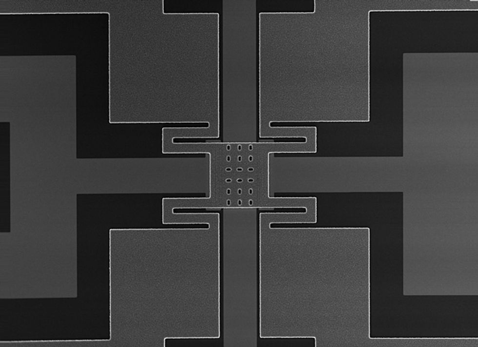
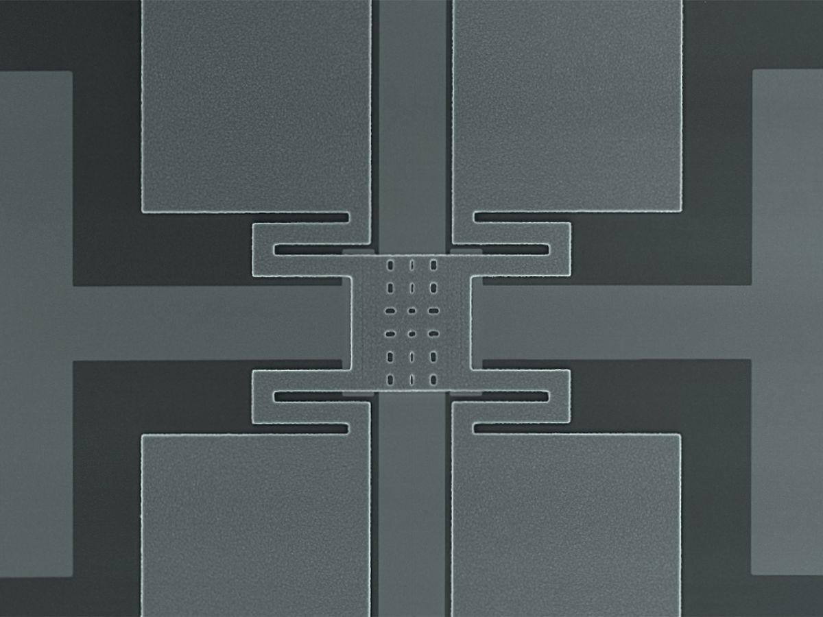
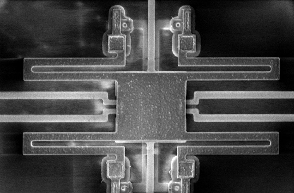
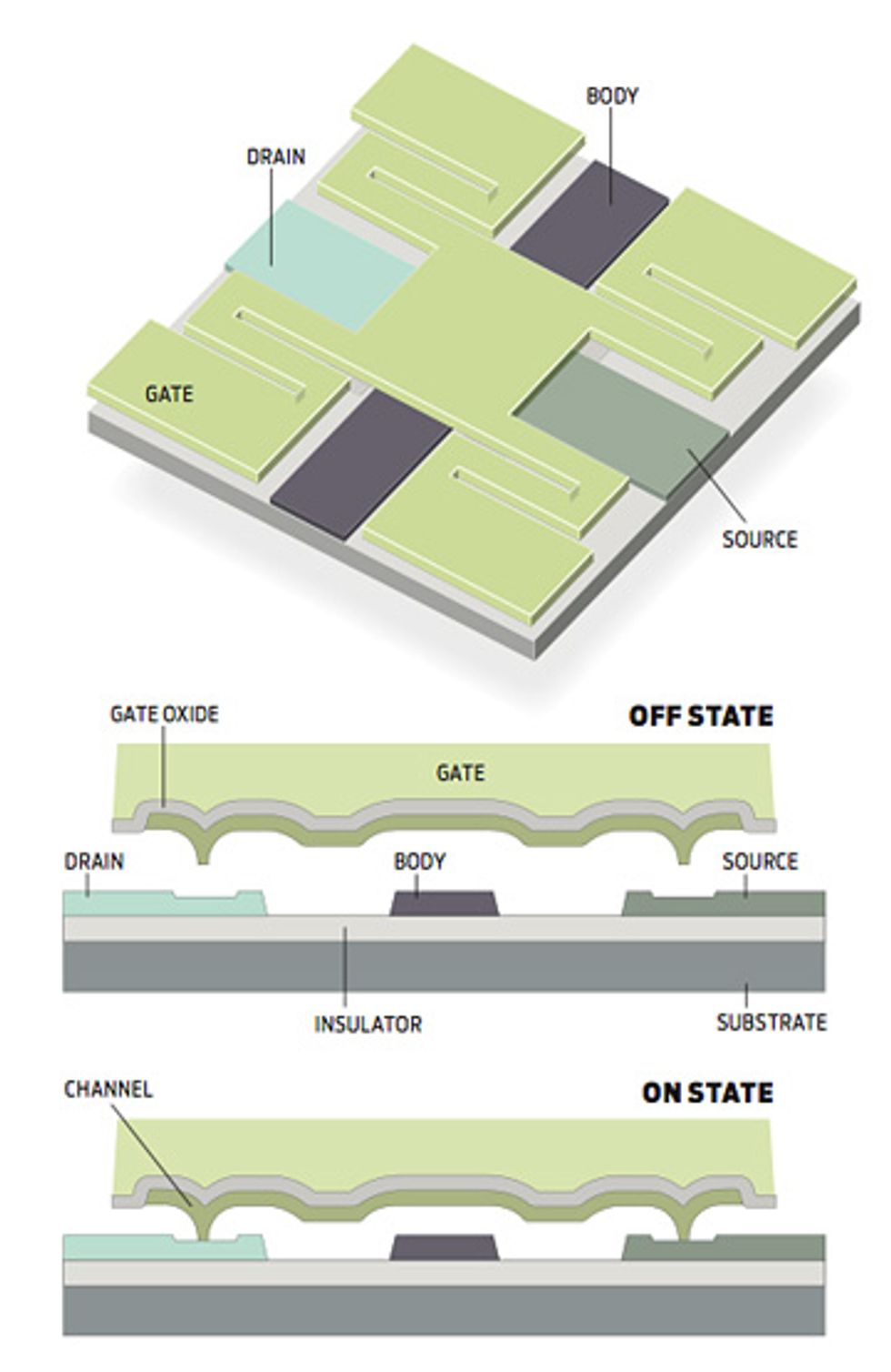
At the University of California, Berkeley, we’ve been working on such a switch: a micrometer-scale relay inspired by the CMOS transistor. Like a transistor, the relay contains a source, a drain, and a channel through which current flows, as well as gate and body electrodes that control the device’s state. But the relay boasts a key structural difference: The gate and channel are suspended above the source and drain rather than built alongside them.
We achieved this configuration by etching the gate—which consists of a square and four springy suspension coils attached at the corners—out of a conductive silicon germanium alloy. Because we cleared away some of the intervening material during the device fabrication process, the gate is suspended less than 100 nanometers above the “base” of the switch. This base is divided into three parts—a “body” electrode that serves as a reference potential for the gate, and source and drain electrodes located on either side of the body electrode. Attached to the insulated underbelly of the gate is a layer of conductive material that forms the channel.
If the voltage difference between the gate electrode and the body electrode is sufficiently large, then the electrostatic attraction between the opposite charges on the gate and body exerts a force that pulls the gate down. This stretches the springy coils and brings the channel into contact with the source and drain electrodes so that it forms a conductive bridge for current to flow through. When the applied voltage between the gate and the body is lowered, the electrostatic force is reduced and eventually becomes lower than the restoring force of the coils. The gate is then pulled back to a neutral position so that it’s once again suspended above the body of the switch. In that state, an air gap separates the channel from the source and drain electrodes, preventing current from flowing.
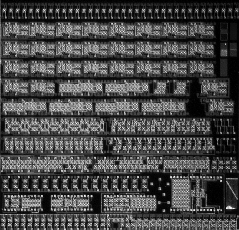
Fortunately, our research team—which includes members at Berkeley, UCLA, and MIT—has demonstrated that the effect of this long mechanical delay can be minimized by optimizing the circuit design. In a CMOS circuit like an adder or multiplier, the transistors are typically arranged in small groups to make fairly simple logic gates. Each of these gates contains a handful of transistors and operates in sequential order—the output of one gate is used to influence the state of the next gate. This approach ends up being speedier than building more-complex logic gates out of large collections of transistors connected in series or in parallel.
It turns out that the best way to design a digital relay circuit block is to take a page from the first half of the 20th century, when large discrete relays were still used to build computers. Instead of grouping the nanorelays into discrete simple gates, as you would do with transistors, the best approach is to arrange many of them in series and in parallel to make as few gates as possible. If all the devices can be arranged into one single gate, all the nanorelays can be switched simultaneously, and the time required to perform any function is reduced to a single mechanical delay.
This approach works because the extra delay associated with the movement of electrical signals through more-complex circuits remains minuscule compared to the mechanical delay associated with opening or closing a single switch. When combined with other relay features, logic circuits built this way require fewer devices, saving space and thus chip cost. While a CMOS adder might require 25 or so transistors, we’ve built nanorelay adders that need only 12 switches. The mechanical circuits that have been fabricated to date contain relays that are micrometer-size, dozens of times as big as today’s highest-performance transistors. But our research—as well as studies by teams at Stanford and Caltech—indicates that relays can be shrunk in a way that’s similar to what’s been done for CMOS transistors, and with similar gains in performance.
Extrapolating from our current relays, our simulation results indicate that for the same lithographic dimensions, a nanorelay circuit could consume as little as a hundredth of the energy while occupying the same chip area as that of an equivalent CMOS circuit. We estimate that nanorelay circuits made using mature 90-nm chip technology could operate at speeds up to about 100 megahertz.
In these days of multiple-gigahertz processors, it might seem strange to contemplate an entirely new technology that’s capable of only about a tenth of the speed. But that amount of computing power is more than enough to drive the logic behind the various sensors, cameras, implanted electronics, and communication devices that will form the future Internet of Things.
And as the nanorelays get smaller, both their energy efficiency and their speed will continue to improve, potentially up to speeds of a gigahertz or so. The best way to boost the speed will be to reduce the mechanical delay of the relays. We could, for example, make the relay’s gate and channel out of lighter materials so that the switch will accelerate faster for a given force. We could also build the relay so that the gate is suspended closer to the body of the switch, reducing the distance a nanorelay gate must travel between its on and off states and boosting the attractive force between the electrodes.
It all sounds straightforward enough, but we’d be remiss if we didn’t mention a couple of caveats. One question we’re often asked is: What would happen to a relay chip if you dropped it? Probably nothing. It turns out that the mass of the movable electrode in a nanorelay would be so small—on the order of a billionth of a gram—that accelerations in excess of 100 000 g’s would be required to overcome the restoring force on the movable electrode springs and cause the channel to accidentally come into contact with the source and drain. To put this number into context, dropping your cellphone on the ground typically results in less than 1000 g’s of acceleration at the moment of impact. Thus it is extremely unlikely that vibrations and mechanical shock would cause a relay chip to fail, let alone damage it—unless your phone happens to explode into pieces.
Another issue is reliability. Any mechanical device will eventually wear out or break with repeated use. In the case of the nanorelay, the most likely way the device will break down is through the contacts—the spots where the channel comes into contact with the source and the drain. The heat created as these contacts conduct current to charge or discharge the output of the relay can eventually cause the contacts to become welded together or even to vaporize.
Conveniently, though, the relative sluggishness of the nanorelay lets us use materials that are more resistant to wear. The electrical delay associated with charging and discharging a switch when a channel comes into contact with or is lifted off the source and drain is tiny compared to the mechanical switching time. As a result, we are free to use more wear- and heat-resistant materials like tungsten for the contacts. Such hard materials don’t make good electrical contacts—they don’t deform when pressed into one another, so actual contact is usually made at only a few points. The resulting small contact area increases the electrical delay, but that delay is still small compared to the mechanical delay.
Extrapolating from the amount of wear seen in our experiments, we estimate that nanorelays could be used to make a practical microcontroller for an embedded sensor that switches a quadrillion (10 15) times without failing. That level of activity corresponds to running 1 percent of the time at speeds of 100 MHz for 10 years.
Furthermore, we expect that as relays are scaled down, they’ll likely become even more reliable. One key reason is that smaller relays will have lower capacitance, which means it will take less time for components to charge or discharge. That will reduce the amount of heat that’s dissipated through the contacts.
Before relays can become the next mainstream integrated circuit technology, two critical things still need to happen: The relays need to get smaller, and they need to be fabricated into more-complex circuits. A number of teams are working on both tasks. We’ve already shown that memory, as well as basic logic circuits such as adders and multipliers, can be built with nanorelays. The next step is to build full chips like microcontrollers, which would easily contain thousands or even millions of switches. In the process, we’ll develop techniques to optimize the design of very-large-scale integrated circuits and also get the wafer fabrication chain ready for those large chip designs.
Fortunately, creating integrated circuits containing millions or even billions of these nanorelays should be relatively uncomplicated. Apart from some relay-specific design rules, checks, and device models, we’ve been able to use the same computer-assisted design tools developed for the silicon CMOS industry to place and route relays and simulate circuit behavior. Being able to reuse this software is critical, because rebuilding this infrastructure from scratch would be very expensive.
Much work remains to be done, of course, but nanorelay technology appears to have the potential to break through the CMOS energy-efficiency roadblock and restore the manifest destiny of electronics. Before long, we may see cool new devices that operate for weeks or years on a single battery charge. All it will take is for a few million things to click into place.
About the Authors
For Tsu-Jae King Liu, Dejan Marković, Vladimir Stojanović, and Elad Alon the relay is more than a blast from the past. IEEE Fellow Liu, a professor of electrical engineering and computer sciences at the University of California, Berkeley, suspected that miniature versions of the mechanical switches could be an attractive, low-power alternative to silicon transistors, but she needed circuit designers to help prove it. Marković, an electrical engineering professor at the University of California, Los Angeles; Stojanović, a professor at MIT; and Alon, a fellow Berkeley professor, all eagerly joined the effort.
