
After more than 50 years of miniaturization, the transistor could stop shrinking in just five years. That is the prediction of the 2015 International Technology Roadmap for Semiconductors (ITRS), which was officially released in July.
After 2021, the report forecasts, it will no longer be economically desirable for companies to continue traditional transistor miniaturization in microprocessors. Instead, chip manufacturers will turn to other means of boosting density, namely turning the transistor geometry from horizontal to vertical and building multiple layers of circuitry, one on top of another.
For some, this change will likely be interpreted as another death knell for Moore’s Law, the repeated doubling of transistor densities that has given us the extraordinarily capable computers we have today. Compounding the drama is that this is the last ever ITRS report, the end to a coordinated planning effort that began in the United States in 1993 and was then expanded to include the rest of the world.
Citing waning industry participation and an interest in pursuing other initiatives, the Semiconductor Industry Association—a U.S. trade group representing the interests of IBM, Intel, and other companies in Washington, D.C., and a key ITRS sponsor—will do its own work, in collaboration with another industry group, the Semiconductor Research Corp., to identify research priorities for government- and industry-sponsored programs. Other ITRS participants are expected to continue with a new road-mapping effort under a new name, which will be conducted as part of an IEEE initiative called Rebooting Computing.
These road-mapping shifts may seem like trivial administrative changes. But “this is a major disruption, or earthquake, in the industry,” says Dan Hutcheson, CEO of the market analysis firm VLSI Research, based in San Jose, Calif. Semiconductor companies in the United States had reason to cooperate and identify common needs in the early 1990s, at the outset of the road-mapping effort that eventually led to the ITRS’s creation in 1998. Suppliers had a hard time identifying what the semiconductor companies needed, he says, and it made sense for chip companies to collectively set priorities to make the most of limited R&D funding.
But the difficulty and expense associated with maintaining the leading edge of Moore’s Law has since resulted in significant consolidation. By Hutcheson’s count, 19 companies were developing and manufacturing logic chips with leading-edge transistors in 2001. Today, there are just four: GlobalFoundries, Intel, Samsung, and TSMC. (Until recently, IBM was also part of that cohort, but its chip fabrication plants were acquired by GlobalFoundries.)
These companies have their own road maps and can communicate directly to their equipment and materials suppliers, Hutcheson says. What’s more, they’re fiercely competitive. “They don’t want to sit in a room and talk about what their needs are,” he says. “It’s sort of like everything’s fun and games when you start off at the beginning of the football season, but by the time you get down to the playoffs it’s pretty rough.”
“The industry has changed,” agrees Paolo Gargini, chair of the ITRS, but he highlights other shifts. Semiconductor companies that no longer make leading-edge chips in-house rely on the foundries that make their chips to provide advanced technologies. What’s more, he says, chip buyers and designers—companies such as Apple, Google, and Qualcomm—are increasingly dictating the requirements for future chip generations. “Once upon a time,” Gargini says, “the semiconductor companies decided what the semiconductor features were supposed to be. This is no longer the case.”
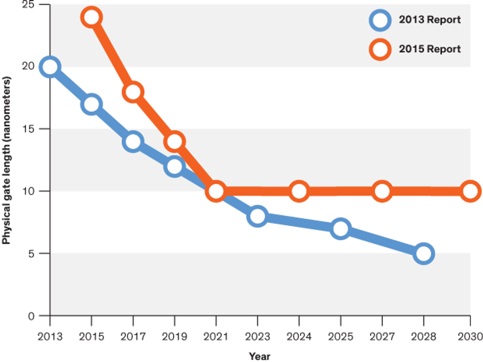 End of The Road: ITRS had previously predicted that the physical gate length of transistors would shrink until at least 2028 (see blue line). The last ITRS report shows this feature size going flat in the coming years. But ITRS chair Paolo Gargini says that some further scaling may be possible after transistors go vertical.
This final ITRS report is titled ITRS 2.0. The name reflects the idea that improvements in computing are no longer driven from the bottom up, by tinier switches and denser or faster memories. The report takes a more top-down approach, focusing on the applications that now drive chip design, such as data centers, the Internet of Things, and mobile gadgets.
The new IEEE road map—the International Roadmap for Devices and Systems (IRDS)—will also take this approach, but it will add computer architecture to the mix, allowing for “a comprehensive, end-to-end view of the computing ecosystem, including devices, components, systems, architecture, and software,” according to a recent press release.
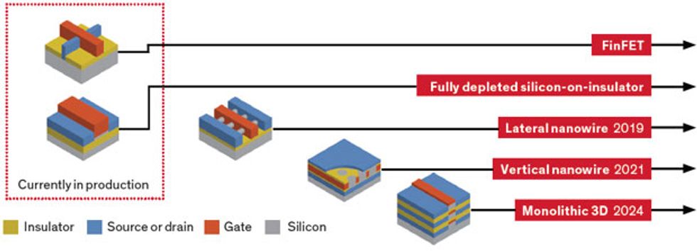 New Geometry: Eventually, miniaturization may be supplanted by monolithic 3D integration, which would build layers of devices, such as the planar transistors shown here, atop one another, connected by dense wiring. Older technologies will continue to be used.
Transistor miniaturization was still a part of the long-term forecast as recently as 2014, when the 2013 ITRS report, the penultimate road map, was released. That report predicted that the physical gate length of transistors—an indicator of how far current must travel in the device—and other key logic-chip dimensions would continue to shrink until at least 2028. But since then, 3D concepts have gained momentum. The memory industry has already turned to 3D architectures to ease miniaturization pressure and boost the capacity of NAND flash. Monolithic 3D integration, which would build layers of devices one on top of another, connecting them with a dense forest of wires, has been an increasingly popular subject of discussion.
The new report embraces these trends, predicting an end to traditional scaling—the shrinking of chip features—by the early 2020s. But the idea that we’re now facing an end to Moore’s Law “is completely wrong,” Gargini says. “The press has invented multiple ways of defining Moore’s Law, but there is only one way: The number of transistors doubles every two years.”
Moore’s Law, he emphasizes, is simply a prediction about how many transistors can fit in a given area of IC—whether it’s done in a single layer, as it has been for decades, or by stacking multiple layers. If a company really wanted to, Gargini says, it could continue to make transistors smaller well into the 2020s, “but it’s more economic to go 3D. That’s the message we wanted to send.”
There are other changes on the horizon. In the coming years, before 3D integration is adopted, the ITRS predicts that leading-edge chip companies will move away from the transistor structure used now in high-performance chips: the FinFET. This device has a gate draped around three sides of a horizontal, fin-shaped channel to control the flow of current. According to the road map, chipmakers will leave that in favor of a lateral, gate-all-around device that has a horizontal channel like the FinFET but is surrounded by a gate that extends underneath as well. After that, transistors will become vertical, with their channels taking the form of pillars or nanowires standing up on end. The report also predicts that traditional silicon channels will be replaced by channels made with alternative materials, namely silicon germanium, germanium, and III-V compounds (drawn from groups 13 and 15 in the current version of the periodic table).
These changes will allow companies to pack more transistors in a given area and so adhere to the letter of Moore’s Law. But keeping to the spirit of the law—the steady improvement in computing performance—is another matter.
The doubling of transistor densities hasn’t been linked to improvements in computing performance for some time, notes Tom Conte, the 2015 president of the IEEE Computer Society and a coleader of the IEEE Rebooting Computing Initiative.
For a long time, shrinking transistors meant faster speeds. But in the mid-1990s, Conte says, the extra metal layers needed to wire up increasing numbers of transistors were adding significant delays, and engineers redesigned chip microarchitectures to improve performance. A decade later, transistor densities were so high that their heat limited clock speeds. Companies began packing multiple cores on chips to keep things moving.
“We’ve been living in this bubble where the computing industry could rely on the device side to do their job, and so the computer industry and the device industry really had this very nice wall between them,” says Conte. “That wall really started to crumble in 2005, and since that time we’ve been getting more transistors, but they’re really not all that much better.”
This crumbling wall was a strong motivation for the IEEE Rebooting Computing Initiative to begin collaborating with the ITRS last year, before the launch of the IRDS. “I like to say we could see the light at the end of the tunnel, and we knew it was an oncoming train,” says Conte.
The initiative held a summit last December that covered a gamut of potential future computing technologies, including new kinds of transistors and memory devices, neuromorphic computing, superconducting circuitry, and processors that use approximate instead of exact answers.
The first international Rebooting Computing conference will be held in October this year; IRDS meetings will coincide with such events, Conte says. The IRDS will still track “Moore’s Law to the bitter end,” Conte explains. But the road-mapping focus has changed: “This isn’t saying this is the end of Moore’s Law,” he says. “It’s stepping back and saying what really matters here—and what really matters here is computing.”
A correction to this article was made on 9 September 2016.


