
Ever since a new class of materials called topological insulators was first created—a discovery that helped win the Nobel Prize in Physics in 2016—researchers have been intrigued by the possibilities for electronics applications such as ultralow-energy transistors, cancer-scanning lasers, and free-space communication beyond 5G. Topological insulators’ unusual name stems from their being insulating on the inside and conductive on the outside: On the outer boundaries of a topological insulator, electricity or (in some cases) light flows readily around corners and defects, and with virtually no losses.
Amazingly, topological insulators appear to be only the first of a possible generation of exotic electrical and optical semimetals, superconductors, and other forms of matter. As confusing as these strange and sometimes outlandish compounds might be at the moment, researchers have found that these materials can possess exceptional properties that could be developed into future technologies.
Topology is the branch of mathematics that explores the nature of shapes independent of deformation. For instance, an object shaped like a doughnut can be deformed into the shape of a mug, so that the doughnut’s hole becomes the hole in the cup’s handle. However, the object couldn’t lose the hole without changing into a fundamentally different shape.
Employing insights from topology, researchers developed the first electronic topological insulators in 2007. Electrons zipping along the edges or surfaces of these materials are “topologically protected,” meaning that the patterns in which the electrons flow will stay unchanged in the face of any disturbances they might encounter.
How might topological materials find their way into the electronics and photonics of tomorrow? Below are a few possible routes.
Electronic topological insulators
Scientists in Australia suggest that transistors based on electronic topological insulators could help computers save substantial amounts of energy. “We expect that topological transistors could replace conventional semiconductor transistors and use much less energy for the same size transistor,” says physicist Michael Fuhrer at Monash University, in Melbourne.
To represent data as ones and zeroes, electronics switch transistors between one electric state and the other, and this switching requires a minimum amount of voltage. The researchers explored replacing the conventional semiconductors used to make transistors with electronic topological insulators. When these materials behave as they normally do, their conductive edges can function as a transistor’s “on” state. But when an electric field is applied, they stop acting like electronic topological insulators and so no longer possess conductive edges, thus serving as a transistor’s “off” state.
By using the right topological materials, the scientists calculated that topological transistors could consume just half the voltage and one-quarter the energy of standard transistors. “Computing today uses 8 to 10 percent of the world’s electricity, and is doubling every decade,” Fuhrer says. “So we need a new technology to make computer chips more efficient. Topological transistors could do this.”
One possible candidate for topological transistors is bismuthene, a single layer of bismuth atoms arranged in a honeycomb lattice. Researchers have only just begun studying bismuthene in the laboratory, so it hasn’t made it into transistors yet. Other materials have not yet been synthesized. “This work takes a lot of time, and we don’t expect that the transistors we envision will be in your iPhone next year, or perhaps even in this decade,” Fuhrer says.
Photonic topological insulators
In 2009, scientists developed photonic topological insulators, in which light is similarly topologically protected. The structures of these materials lead specific wavelengths of light to flow along their outsides without losses or scattering, even around corners and imperfections.
The first topological insulators to find practical use may in fact be photonic, not electronic. One possible application could be lasers that incorporate topological protection, which may display significantly better efficiency and robustness against defects than conventional devices. Such benefits will boost the number and consistency of usable devices after fabrication, says electrical and optical engineer Qi Jie Wang at Nanyang Technological University, in Singapore.
The scientists began with a wafer made of layers of gallium arsenide and aluminum gallium arsenide. When electrically charged, the wafer emitted bright light. The researchers drilled an array of holes into the wafer, each resembling an equilateral triangle with its corners trimmed off. Around this lattice the researchers drilled additional holes of the same shape but oriented in the opposite direction. The light from the wafer flowed along the boundary between the different sets of holes and emerged from nearby channels as laser beams. This flow proved robust against defects, including the extra holes the scientists drilled. “We are able to create photonic structures that light can pass through without scattering losses or reflections,” Wang says.
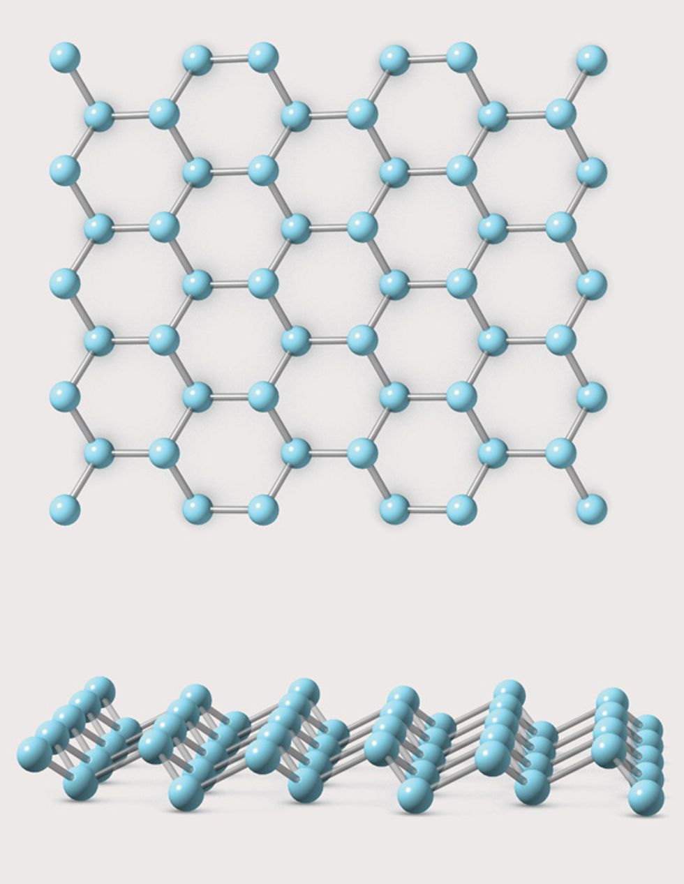 Bismuthene, a single layer of bismuth atoms in a honeycombed sheet, could be the stuff of future topological transistors.Emily Cooper
This laser works in terahertz frequencies, which are useful for cancer screening and airport security scans. Wang and his colleagues are currently exploring topological lasers using layers of indium gallium arsenide and indium aluminum arsenide sandwiched together to emit mid-infrared wavelengths, useful for applications such as detecting and analyzing air pollutants, lidar sensors, or free-space communication beyond 5G. He notes that the COVID-19 pandemic has delayed experimental work, however.
Topological superconductors
Whereas topological insulators possess topologically protected electrons or photons on their exteriors, an unusual class of superconductors known as topological superconductors may boast elusive theoretical particles on their surfaces that could drive a major advance in quantum computing.
Topological superconductors are often made of a superconducting metal coupled with a semiconductor. Interactions between these materials can generate Majorana fermions, long-theorized particles that are their own antiparticles.
Majorana fermions could find use as quantum bits, or qubits, which lie at the heart of most quantum computers—machines that can theoretically perform more computations in an instant than there are atoms in the universe. Qubits are typically fragile, but the Majorana fermions of topological superconductors could prove topologically protected against disturbances, a feature that scientists have suggested could lead to a practical quantum computer. “Topological qubits are the most important reason people are interested in topological superconductivity,” says condensed-matter theorist Ruixing Zhang at the University of Maryland, College Park.
However, so far no conclusive proof has emerged for the existence of either topological superconductors or Majorana fermions, Zhang says. A 2018 Microsoft-backed study claimed to find strong evidence of both, but this work was ultimately retracted in 2021.
Still, researchers hold out hopes of confirming the existence of topological superconductors. Zhang and his colleagues suggest examining thin films of iron-based superconductors, while others suggest materials such as graphene. “I’m very optimistic we’ll realize Majorana physics in the coming years,” Zhang says.
Topological semimetals
Topological semimetals sit between metals and insulators in terms of such properties as their ability to conduct electricity or heat. Increasingly, scientists around the world find that these materials can possess extraordinary features, such as virtually dissipationless electric currents and the ability to convert more light to electricity than any other material can, which hint at a wide range of potential applications, such as ultralow-power electronics and generating electricity from waste heat.
A dizzying variety of topological semimetals exist, such as Dirac semimetals, Weyl semimetals, multifold fermion semimetals, and more, each of which are topologically different from the others. Whereas conventional semimetals can easily convert to either metals or insulators with a change in temperature or a slight tweak of their chemical makeup, topological semimetals stubbornly retain their semimetallic nature despite changes to temperature or composition.
Just like graphene, electric currents can flow in topological semimetals with virtually zero dissipation of energy, potentially making them useful for ultralow-power electronics, says physicist Masaki Uchida at the Tokyo Institute of Technology. At the same time, researchers can theoretically vary the thicknesses of topological semimetals to tune their properties, whereas atomically thin graphene has finite thickness and thus less flexibility for design purposes, says physicist Yee Sin Ang at the Singapore University of Technology and Design.
Topological semimetals can also display unexpected properties—for example, physicist Ken Burch at Boston College and his colleagues found that tantalum arsenide can intrinsically generate more than 10 times as much electric current from light as any other material. This effect occurs with mid-infrared light, which suggests that tantalum arsenide could find use in chemical and thermal imaging. “You could also imagine taking infrared radiation emitted as waste energy off hot objects and converting it to useful electricity,” Burch says.
Scientists may have overlooked the dramatic features of many topological semimetals for decades. Theoretical physicist Benjamin Wieder at MIT and his colleagues just recently discovered such properties in cobalt monosilicide and similar materials, which researchers have studied for nearly 70 years.
“The future of topological materials discovery and applications might not be in the design of new materials, but in...the rediscovery of interesting materials with overlooked properties,” Wieder says. “The next highly desirable solid-state material might be hiding in a 70-year-old paper, if you know where to look.”
- A Transistor for Sound Points Toward Whole New Electronics - IEEE Spectrum ›
- Topology can Protect Qubits in Photonic Chips ›
- Qubits’ Entanglement Must be Protected—is the Answer Math? ›
- AI Blazes Path Towards Dissipationless Electronics - IEEE Spectrum ›
- Photonic Topological Insulator May Boost 5G, Radar ›
- Hydrogen Could Help Make Topological Insulators Practical ›
- Magnetic Knots Push Future Computing Toward 3D - IEEE Spectrum ›
- In "Strange Metals," the Flow of Electricity Is Equally Strange - IEEE Spectrum ›
- Ultrasound Circuit: Topological Device Could Cut IoT Interference - IEEE Spectrum ›


