Novel devices known as photonic topological electromagnetic circuits may one day support 5G wireless broadband networks and advanced radar systems, a new study finds.
Topology is the branch of mathematics that explores what features of shapes may survive deformation. For instance, an object shaped like a doughnut can be deformed into the shape of a mug, so that the doughnut’s hole forms the hole in the cup’s handle. However, the object couldn’t lose its hole without changing into a fundamentally different shape.
Employing insights from topology, researchers developed the first electronic topological insulators in 2007. Electrons zipping along the edges or surfaces of these materials are “topologically protected,” meaning that the patterns in which the electrons flow will stay unchanged in the face of any disturbances they might encounter, a discovery that helped win the Nobel Prize in Physics in 2016.
Scientists later designed photonic topological insulators, in which light is similarly protected. One possible application for such materials could be lasers that incorporate topological protection, which may be significantly more efficient and robust against defects than conventional devices. Another is helping data travel across chips at a trillion bits per second.
The useful properties of photonic topological insulators usually arise from regular variations in their structures. These let specific wavelengths of light flow along the exterior of the materials without scattering or losses, even around corners and imperfections.
However, this approach to generating photonic topological protection has a number of drawbacks. One issue is that the size of these structural variations is at least half that of the wavelengths they are manipulating. This can not only make these materials bulky, but also limit the range of wavelengths they can target.
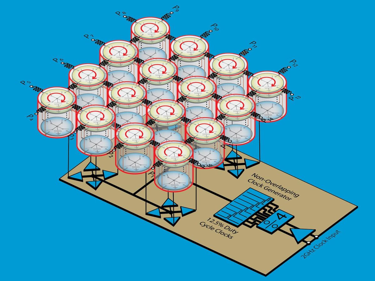
In the new study, instead of creating a photonic topological insulator whose properties depend on how a material’s structure varies in space, researchers created a device whose properties vary over time. It consists of a square lattice of 16 identical units, each of which are made of eight capacitors that can be switched on and off in patterns that result in each unit’s electric field rotating in a spiraling manner.
The main benefit of this new photonic topological electromagnetic circuit is how its units are each far smaller than the wavelengths they target, making it 100 to 1,000 times more compact than earlier photonic topological insulators. In addition, it can manipulate a much broader range of wavelengths than previous devices, spanning up to gigahertz frequencies.
“I am particularly excited by the enormous enhancement in bandwidth for a photonic topological insulator that we have been able to demonstrate, and at the same time the enormous reduction in footprint,” says study co–senior author Andrea Alù, an electrical engineer at the City University of New York’s Graduate Center. “I believe these two advances bring the whole field of photonic topological insulators much closer to applications and impact.”
Alù and his colleagues integrated their new 3.5- by 3.4-millimeter device onto a CMOS chip that enabling them to reconfigure the circuitry in real time. Electromagnetic waves could travel in a topologically protected manner without dispersion along the boundary of the device.
The researchers investigated how the new device might perform as an antenna interface for a 5G wireless system. The full-duplex phased-array system they experimented with can potentially combine the benefit of double capacity with the multiplexing gains of multiple-antenna systems. Traditionally, these systems often struggle with the complex interference that can occur within each pair of transmitters and receivers.
The scientists found their device could help each of the eight antennas in the 730-megahertz full-duplex phased-array system operate independently and simultaneously in an isolated manner. This helped suppress interference between the antennas and enabled simultaneous transmission and reception of broadband radio signals to enhance their data rates.
Alù and his colleagues also experimented their new device as the antenna interface in an ultrawideband impulse radar system. An impulse radar scans areas with brief, weak radio signals over a large bandwidth, a strategy that results in minimal interference with other wireless systems as well as high immunity to nearby radio signals.
The challenges of sending and receiving radar signals over a large bandwidth often leads conventional ultrawideband impulse radars to struggle with noise or large sizes or both. In experiments, the new photonic topological insulator could help an ultrawideband impulse radar array shape the beams from multiple transmitters and receivers in a way that could enable a much smaller and less noisy system.
“We are very excited by the prospects of applying these findings to wireless communication and radar systems,” Alù says. In addition, photonic topological insulators may find use in more robust, fault-tolerant quantum computers, the researchers say.
The scientists detailed their findings online on 2 May in the journal Nature Electronics.
- Is Math the Key to Quantum Entanglement Protection? - IEEE ... ›
- Novel Materials Could Help Terahertz Chips Deliver Data at Terabits ... ›
- A Beginner's Guide to Topological Materials - IEEE Spectrum ›
- Experiment Reveals the Peculiar Way Light Travels in a Photonic ... ›
- Topological Photonics: What It Is and Why We Need It - IEEE Spectrum ›
- Hydrogen Could Help Make Topological Insulators Practical ›
- Strange Topological Physics Could Help Enable 6G Tech - IEEE Spectrum ›
Charles Q. Choi is a science reporter who contributes regularly to IEEE Spectrum. He has written for Scientific American, The New York Times, Wired, and Science, among others.


