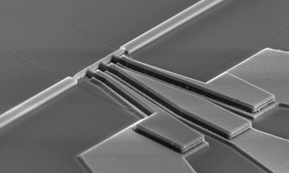
Fiber optic links are already the main method of slinging data between clusters of computers in data centers, and engineers want to bring their blazing bandwidth to the processor. That step comes at a cost that researchers at the University of Toronto and Arm think they can greatly reduce.
Silicon photonics components are huge in comparison to their electronic counterparts. That’s a function of optical wavelengths being so much larger than today’s transistors and the copper interconnects that tie them together into circuits. Silicon photonic components are also surprisingly sensitive to changes in temperature, so much so that photonics chips must include heating elements that take up about half of their area and energy consumption, as Charles Lin, one of the team at University of Toronto, explained last month at the IEEE International Electron Device Meeting.
At the virtual conference Lin, a researcher in the laboratory of Amr S. Helmy, described new silicon transceiver components that dodge both of these problems by relying on plasmonics instead of photonics. The results so far point to transceivers capable of at least double the bandwidth while consuming only one third the energy and taking up a mere 20 percent of the area. What’s more, they could be built right atop the processor, instead of on separate chiplets as is done with silicon photonics.
When light strikes the interface between a metal and insulator at a shallow angle, it forms plasmons: waves of electron density that propagate along the metal surface. Conveniently, plasmons can travel down a waveguide that is much narrower than the light that forms it, but they typically peter-out very quickly because the metal absorbs light.

The Toronto researchers invented a structure to take advantage of plasmonics’ smaller size while greatly reducing the loss. Called the coupled hybrid plasmonic waveguide (CPHW), it is essentially a stack made up of silicon, the conductor indium tin oxide, silicon dioxide, aluminum, and more silicon. That combination forms two types of semiconductor junctions—a Schottky diode and a metal-oxide-semiconductor—with the aluminum that contains the plasmon in common between the two. Within the metal, the plasmon in the top junction interferes with the plasmon in the bottom junction in such a way that loss is reduced by almost two orders of magnitude, Lin said.
Using the CPHW as a base, the Toronto group built two key photonics components—a modulator, which turns electronic bits into photonic bits, and a photodetector, which does the reverse. (As is done in silicon photonics, a separate laser provides the light; the modulator blocks the light or lets it pass to represent bits.) The modulator took up just 2 square micrometers and could switch at as fast as 26 gigahertz, the limit of the Toronto team’s equipment. Based on the device’s measured capacitance, the real limit could be as high as 636 GHz. The plasmonic photodetector was near match to silicon photonics’ sensitivity, but it was only 1/36th the size.
One of the CPHW’s biggest advantages is its lack of sensitivity to temperature. Silicon photonics components have a temperature tolerance that can’t swing farther than one degree in order for them to operate at the proper wavelength. Temperature sensitivity is a “big challenge for silicon photonics,” explains Saurabh Sinha, a principal research engineer at Arm. Managing that tolerance requires both extra circuitry and the consumption of energy. In a simulated 16-channel silicon photonics transceiver heating circuits consume half of the circuit’s energy and take up nearly that fraction of their total area, and that translates to huge difference in area: 0.37 mm2 for silicon photonics versus 0.07 mm2 for plasmonic transceivers.
Simulations of the CPHW-based plasmonics transceiver predict a number of benefits over silicon photonics. The CPHW system consumed less than one-third of the energy per bit transmitted of a competing silicon photonics system—0.49 picojoules per bit versus 1.52 pJ/b. It could comfortably transmit more than three times more bits per second at acceptable Ethernet error rates without relying on error correction—150 gigabits per second versus 39 Gb/s.
Sinha says Arm and the Toronto group are discussing next steps, and those might include exploring other potential benefits of these transceivers such as the fact that CPHWs could be constructed atop processor chips, while silicon photonics devices must be made separately from the processor and then linked to them inside the processor package using chiplet technology.
Samuel K. Moore is the senior editor at IEEE Spectrum in charge of semiconductors coverage. An IEEE member, he has a bachelor's degree in biomedical engineering from Brown University and a master's degree in journalism from New York University.


