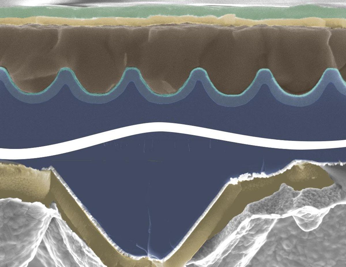
By adding periodic nanostructures that look like egg-crate foam to tandem solar cells made of silicon and perovskites, researchers at the Helmholtz-Zentrum Berlin in Germany have achieved a certified efficiency of 29.8 percent.
This was the world record for tandem solar-cell efficiency until July of this year, when researchers at the Swiss Federal Institute of Technology Lausanne (EPFL) surpassed it slightly, setting a new record of 31 percent. The German team, however, has presented details of how they achieved their milestone efficiency—and insights about how to further the promise of perovskite solar tech—in a recent paper in Nature Nanotechnology.
Silicon solar cells have a theoretical efficiency limit of around 29 percent, with the best cells today reaching efficiencies of just under 27 percent. Solar cells made of III-V semiconductors can achieve efficiencies higher than 30 percent, but those materials are expensive and difficult to process.
Tandem cells, in which silicon is coated with easy-to-make photovoltaic perovskites, offer a way to achieve efficiencies over 40 percent, in theory at least, at low cost and without needing drastically different manufacturing facilities.
Teams working on such tandem devices have so far tried to eke out every little efficiency gain by tweaking the chemical composition of the perovskites, making nicer more uniform layers, and improving the contact between the two material layers, among other tricks.
The German team, and the Swiss team after them, boosted efficiency by creating a texture on the silicon surface. Texturing solar cells reduces reflection losses, which increases the current that the device generates, says Philipp Tockhorn, a researcher at Helmholtz-Zentrum and first author of the new paper. “Textures are essential to tap the full optical potential of perovskite–silicon tandem solar cell and to reduce optical losses to a minimum.”
The standard way to texture silicon-only cells is to create random pyramidal structures that are several micrometers in size. But that doesn’t work for tandem cells because the height of standard pyramidal textures surpasses the thickness of the perovskite layer, Tockhorn says. To overcome that, researchers have tried to either alter the perovskite deposition method while keeping the pyramid texture the same, or tried tweaking the pyramidal textures to more easily deposit perovskite solution on them. “There is a challenge to fully cover the texture without pinholes, which would deteriorate the performance,” he says.
The Swiss EPFL team’s solution was to use a hybrid vapor/solution processing technique that is compatible with pyramidal textured silicon surfaces. They made a 1-square-centimetersolar cell with a power conversion efficiency of 31.25 percent.
But Tockhorn and his colleagues decided to investigate shallower nanotextures. Based on previous experimental work and backed up by optical simulations, the team decided on a sinusoidal design with a hexagonal arrangement. These nanotextures can be easily coated with perovskite without compromising the quality of the perovskite, he says.
Not only did the nanotexturing improve efficiency, it also increased the yield of high-quality tandem solar cells. That’s because the textured surface retained the perovskite solution better than a flat silicon surface, resulting in a better-quality perovskite film. Out of 45 nanotextured tandem solar cells, only two had visible holes after perovskite coating, making for about 95 percent yield. The planar devices had a 50 percent yield: 15 out of 30 devices showed macroscopic holes.
The German group used ultraviolet nanoimprint lithography and etching to make the nanostructured silicon surface. The final perovskite–silicon cell was 1 cm2 in size. The nanoimprint techniques they used are relatively easy to scale up to large area, Tockhorn says. “Many researchers from academia regard nanoimprint lithography as a very promising tool for solar cells due to its sheer simplicity and versality in terms of structure type.”
Now that they have a proof-of-concept demonstration for making solution-based perovskite layers on textured silicon wafers, he says they are working on improving the devices to boost efficiency even further. “We need to aim for a fully textured perovskite top cell, that is textured at the front and at the interface between perovskite and silicon.”
This article appears in the January 2023 print issue as “Perovskite Solar-Cell Efficiency Approaches 30 Percent.”
- A Bright Spot for Solar Windows Powered by Perovskites - IEEE ... ›
- Power From Commercial Perovskite Solar Cells Is Coming Soon ... ›
- Perovskite-Silicon Pair Sails Past 30 Percent - IEEE Spectrum ›
Prachi Patel is a freelance journalist based in Pittsburgh. She writes about energy, biotechnology, materials science, nanotechnology, and computing.


