Currently, LCD HDTV screens operate according to ATC Standards, with 1080 gate lines and refresh rates up to 30 frames per second. Going to higher definition, such as 4000 or 8000 lines and refresh rates up to 240 frames per second, is currently out of reach, both for OLED and LCD screens, because the pixels are driven by thin-film transistors that are simply too slow. Typically, their electron mobility is below 20 square centimeters per volt seconds (cm2/vs). “There is not much time to supply the voltage or the current through the transistor for a high frame rate and high definition display,” says Sanghun Jeon (PDF), a researcher at Korea University in Sejong. “We estimate that for future display technology, the mobility should be exceeding 100 cm2/vs.” Jeon and other researchers at Korea University and at the Samsung Advanced Institute of Technology in Gyeonggi-do, Korea, report this week in Applied Physics Letters the creation of just such a transistor. The one they developed has an electron mobility of 138 cm2/vs.
The transistor consists of a thin film of zinc oxynitride, ZnON, a glassy composite of ZnO, ZnOxNx and Zn3N2. Using sputtering, they deposited a mixture of nitrogen, oxygen, and argon gases onto a zinc target, forming a film 50 nanometers thick. However, because nitrogen bonds weakly with zinc, as compared with oxygen, the layer was susceptible to oxidation when exposed to air. To prevent this, the researchers treated the layer with a high-energy plasma of argon ions. These ions, when they collided with the atoms in the ZnON, rearranged the bonds between atoms, just like shaking a box with colored marbles will result in a redistribution of colors. The process resulted in a chemically uniform layer, more resistant to chemical degradation.
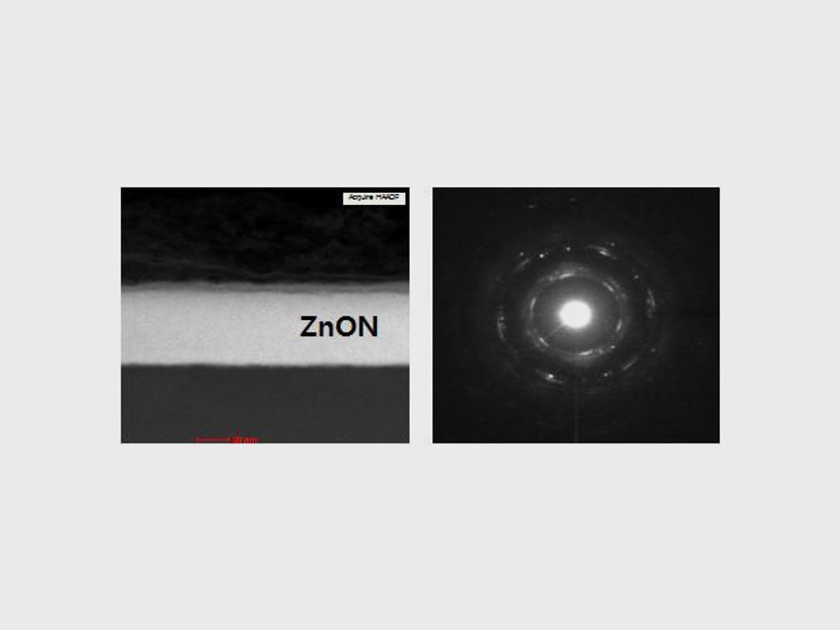
The researchers made scanning transmission electron microscope (STEM) images of an annealed thin film obtained by current production processes with their new experimental thin film. “The STEM image of argon-plasma-treated ZnON material shows uniform contrast throughout the entire film, indicating that the composition of argon-plasma-treated ZnON film is very uniform,” says Jeon. And it is this uniformity that is at the root of the high electron mobility in the ZnON film, explains Jeon, who notes that defects at the interfaces and in the bulk of such semiconductors slow electrons down a lot.
The argon plasma process augurs well for future large scale production, especially because ZnON is known to have poor reproducibility. “We were surprised that by employing the argon process, we were able to reproduce the device well, together with a high mobility constantly exceeding 100 cm2/vs," says Jeon. However, more work is required before the thin-film transistors will control pixels on actual screens. Getting to that point will take two or three more years, says Jeon.


