
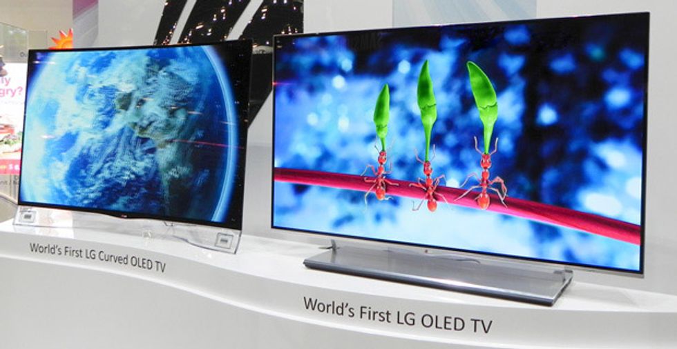
 Look, But Don’t Touch? New display technologies, such as these OLED screens, provide amazing picture quality but have been troubled by manufacturing yield problems.Photo: Alfred Poor
As companies around the world showcased their latest developments, Display Week 2013 proved to be a good bellwether for how next-generation screen technologies were faring in the marketplace. As an extension of the trend toward higher-resolution displays, a lot of attention was focused on 4K displays, which have the same resolution as four standard 1080p HDTVs tiled together. And LG Electronics and Samsung both continued to tout their 55-inch organic light-emitting diode (OLED) television displays, which had been shown before but are now being offered for sale.
One of the themes of this year’s show, run in Vancouver at the end of May by the Society for Information Display, was whether the industry can deliver these next-generation displays in large numbers. Manufacturers cannot yet produce enough units to have viable mass-market products, and they’re spending a lot of time and money to achieve that goal.
Both 4K and large OLED displays suffer from the limitations of today’s silicon-based backplanes. Backplanes serve as the substrates on which thin-film transistors are fabricated. (TFTs turn pixels on and off.) For a given screen size, a 4K display has four times as many pixels as a 1080p panel, so it requires TFTs one-quarter the size. You need a lot of electron mobility in the backplane to support TFT devices that small. Good electron mobility is also critical for OLED displays, even at 1080p resolutions, as the pixels must be driven by more current than with LCDs.
Electron mobility is measured in the somewhat awkward units of square centimeters per volt second (cm2/Vs). Amorphous silicon, with an electron mobility of about 1 cm2/Vs, served LCDs well for years but isn’t suitable for the new displays. Laser annealing of amorphous silicon to turn it into a polycrystalline form, typically in the range of 50 to 150 cm2/Vs, has been the mainstay for high-resolution mobile display manufacture. This process adds costs, however, and does not scale up well. Some manufacturers are making polycrystalline silicon with a so-called low-temperature process. Unfortunately, at large sizes the resulting polysilicon is not uniform, forcing makers to take complex quality control measures.
So manufacturers have been very interested in metal-oxide semiconductor backplanes; the most common type in production today uses a mix of indium, gallium, and zinc oxides. IGZO is a low-cost material that’s easy to deposit on a glass substrate, and it scales up well. Its electron mobility is about 10 to 30 cm2/Vs, sufficient for 4K or OLED displays.
Sharp has invested heavily in this technology and is now shipping LCDs with IGZO backplanes, such as the not-so-romantically named LQ315D1LG91, a 31.5-inch panel with 3840- by 2160-pixel resolution. LG Display is also using metal-oxide TFTs for its planned rollout of 55-inch OLED television sets.
It hasn’t been all smooth sailing for metal oxides, however. Among other problems, the metal-oxide layer is often uneven. This can cause visible differences in performance from one spot to the next in OLED applications. In the worst case, a spike of material can pierce subsequent layers, potentially ruining the whole panel.
Researchers continue to work to counter these shortcomings. Increasing production to reduce prices and provide flawless performance will be essential if large 4K and OLED technologies are to find a place in consumers’ living rooms.
Finally, of the few brand-new technologies shown at Display Week, perhaps the most notable was a flexible, self-organizing, transparent conductive layer that uses silver nanoparticles. A thin paste, made by Cima NanoTech, is applied to a surface, and silver particles within the paste are attracted to one another to form a random network of connections. The result has excellent electrical conductivity and is claimed to be 88 percent transparent. In addition to applications such as touch screens, the material can even be used as a transparent defrosting layer for car windows and is already shipping for some low-volume production items.
About the Author
A speaker and author, Alfred Poor has written thousands of articles over the past 30 years. He is a senior member of the Society for Information Display, and continues to be fascinated and amazed by new developments in screen technology.


