Today at Nvidia’s developer conference, GTC 2024, the company revealed its next GPU, the B200. The B200 is capable of delivering four times the training performance, up to 30 times the inference performance, and up to 25 times better energy efficiency, compared to its predecessor, the Hopper H100 GPU. Based on the new Blackwell architecture, the GPU can be combined with the company’s Grace CPUs to form a new generation of DGX SuperPOD computers capable of up to 11.5 billion billion floating point operations (exaflops) of AI computing using a new, low-precision number format.
“Blackwell is a new class of AI superchip,” says Ian Buck, Nvidia’s vice president of high-performance computing and hyperscale. Nvidia named the GPU architecture for mathematician David Harold Blackwell, the first Black inductee into the U.S. National Academy of Sciences.
The B200 is composed of about 1600 square millimeters of processor on two silicon dies that are linked in the same package by a 10 terabyte per second connection, so they perform as if they were a single 208-billion-transistor chip. Those slices of silicon are made using TSMC’s N4P chip technology, which provides a 6 percent performance boost over the N4 technology used to make Hopper architecture GPUs, like the H100.
Like Hopper chips, the B200 is surrounded by high-bandwidth memory, increasingly important to reducing the latency and energy consumption of large AI models. B200’s memory is the latest variety, HBM3e, and it totals 192 GB (up from 141 GB for the second generation Hopper chip, H200). Additionally, the memory bandwidth is boosted to 8 terabytes per second from the H200’s 4.8 TB/s.
Smaller Numbers, Faster Chips
Chipmaking technology did some of the job in making Blackwell, but its what the GPU does with the transistors that really makes the difference. In explaining Nvidia’s AI success to computer scientists last year at IEEE Hot Chips, Nvidia chief scientist Bill Dally said that the majority came from using fewer and fewer bits to represent numbers in AI calculations. Blackwell continues that trend.
It’s predecessor architecture, Hopper, was the first instance of what Nvidia calls the transformer engine. It’s a system that examines each layer of a neural network and determines whether it could be computed using lower-precision numbers. Specifically, Hopper can use floating point number formats as small as 8 bits. Smaller numbers are faster and more energy efficient to compute, require less memory and memory bandwidth, and the logic required to do the math takes up less silicon.
“With Blackwell, we have taken a step further,” says Buck. The new architecture has units that do matrix math with floating point numbers just 4 bits wide. What’s more, it can decide to deploy them on parts of each neural network layer, not just entire layers like Hopper. “Getting down to that level of fine granularity is a miracle in itself,” says Buck.
NVLink and Other Features
Among the other architectural insights Nvidia revealed about Blackwell are that it incorporates a dedicated “engine” devoted to the GPU’s reliability, availability, and serviceability. According to Nvidia, it uses an AI-based system to run diagnostics and forecast reliability issues, with the aim of increasing up time and helping massive AI systems run uninterrupted for weeks at a time, a period often needed to train large language models.
Nvidia also included systems to help keep AI models secure and to decompress data to speed database queries and data analytics.
Finally, Blackwell incorporates Nvidia’s fifth generation computer interconnect technology NVLink, which now delivers 1.8 terabytes per second bidirectionally between GPUs and allows for high-speed communication among up to 576 GPUs. Hopper’s version of NVLink could only reach half that bandwidth.
SuperPOD and Other Computers
NVLink’s bandwidth is key to building large-scale computers from Blackwell, capable of crunching through trillion-parameter neural network models.
The base computing unit is called the DGX GB200. Each of those include 36 GB200 superchips. These are modules that include a Grace CPU and two Blackwell GPUs, all connected together with NVLink.
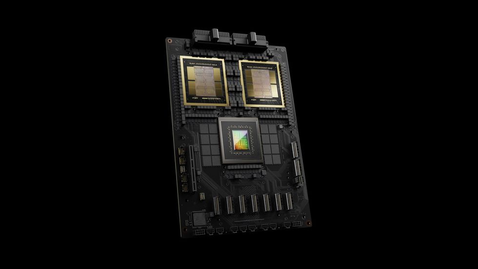 The Grace Blackwell superchip is two Blackwell GPUs and a Grace CPU in the same module.Nvidia
Eight DGX GB200s can be connected further via NVLINK to form a 576-GPU supercomputer called a DGX SuperPOD. Nvidia says such a computer can blast through 11.5 exaflops using 4-bit precision calculations. Systems of tens of thousands of GPUs are possible using the company’s Quantum Infiniband networking technology.
The company says to expect SuperPODs and other Nvidia computers to become available later this year. Meanwhile, chip foundry TSMC and electronic design automation company Synopsys each announced that they would be moving Nvidia’s inverse lithography tool, cuLitho, into production. Lastly, the Nvidia announced a new foundation model for humanoid robots called GR00T.