Researchers at Case Western University have fabricated nanoelectromechanical system (NEMS) resonators made from molybdenum disulfide that have an extraordinarily broad dynamic range. These nanoscale devices’ range is roughly comparable to that of human and animal hearing. The advance could lead to ultra-low-power signal processing and sensing functions in future electronic and optoelectronic chips, according to the researchers.
Dynamic range—the ratio between the highest level of an undistorted signal (“signal ceiling”) over its lowest detectable signal (“noise floor”)—is essential to all sensing and communication, whether it be sensory organs in animals or engineered devices. It’s usually measured in decibels (dB).
In research described in the journal Science Advances, the Case Western researchers, led by Philip Feng, demonstrated that their NEMS resonators have a dynamic range of up to ~110 dB at radio frequencies up to over 120 megahertz. This dynamic range represents the highest reported to date for vibrating resonators made of two-dimensional (2D) materials and other nanoscale structures, says Feng.
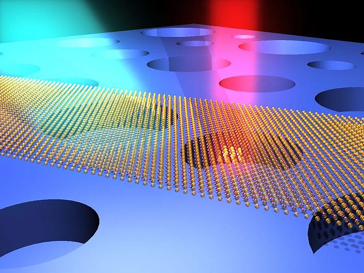
These 2D resonators function like the skin of a drum that vibrates at certain frequencies. When struck by something, such as a molecule or photon, those frequencies change. Measuring those frequency changes makes it possible to identify what has hit the device. You can see a visual representation of how this technology operates in the video below.
In this research, Feng and his team demonstrated that they can also tune the device by stretching the drumhead membranes using electrostatic forces induced by controlling the number of electrons accumulated in the devices, thus providing it with a fairly wide tunability.
“When fully leveraged, this broad dynamic range will translate into high performance in sensitivity for various physical sensors and transducers enabled by such devices, toward real-time sensing applications,” said Feng. “The unique combination of broad dynamic range and frequency tunability also holds promise for making ultralow-power oscillators that could have both low noise performance and excellent tuning capability.”
This is not the first time NEMS resonators have been produced using molybdenum disulfide. In fact, Feng and his research team fabricated just such a device five years ago. However, at that time, no tests were performed to measure the resulting device’s dynamic range, mainly because in order to take measurements at frequencies above 100 MHz at room temperature, ultrasensitive equipment is required.
“These are very ‘quiet’ devices and we have to ‘listen’ to them very carefully and ‘talk’ to them very gently,” said Feng.
When researchers have bothered to measure the dynamic range of nanoscale resonators, the results have been pretty poor. The reason one-dimensional (1D) nanomaterials such as carbon nanotubes (CNTs) and nanowires have such relatively poor dynamic ranges stems from their high thermomechanical fluctuations due to large Brownian motion, the random movement of particles resulting from them bumping into each other. As a result, these materials have high noise floors that narrow their dynamic ranges from the lower boundary side.
The upper boundary of dynamic range, the signal ceiling, is usually based on the onset of signal distortion. The 2D devices also experience distortion later that helps to improve the dynamic range of 2D materials as well.
“2D membranes have broader dynamic ranges than 1D devices because they benefit from both ends–lower noise floor, and higher signal ceiling,” said Feng.
In order to commercialize this technology, Feng foresees that some demanding engineering still needs to be addressed, because 2D NEMS technology is still a quite new area that is in its early stage.
Feng added: “Exciting and challenging topics for us include wafer-scale fabrication and testing of such devices, further engineering on improving device performance, and developing prototype chips for targeted applications in relevant frequency bands.”
Dexter Johnson is a contributing editor at IEEE Spectrum, with a focus on nanotechnology.


