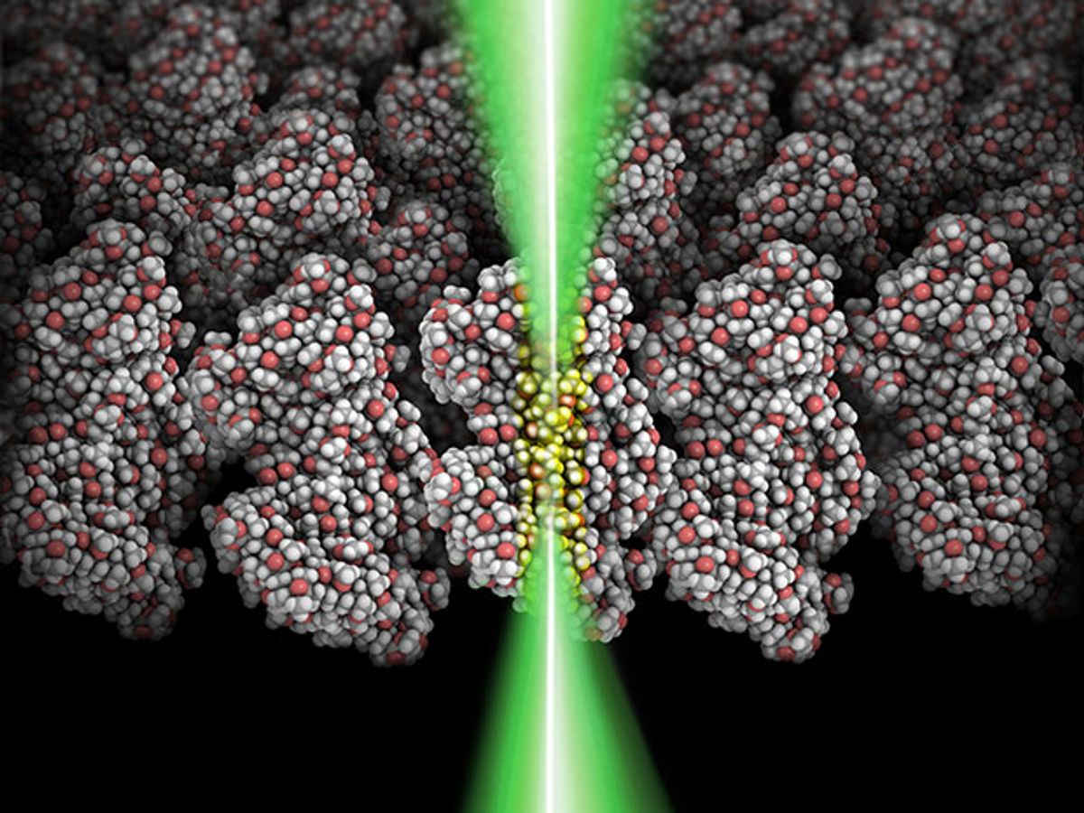
Scientists at the U.S. Department of Energy’s (DOE) Center for Functional Nanomaterials (CFN) at Brookhaven National Laboratory have established a new record in reducing lithographic feature sizes using electron-beam lithography (EBL), which involves exposing an electron-sensitive material to a focused beam of electrons.
In their latest research, described in the journal Nano Letters, the CFN team performed electron beam lithography with a scanning transmission electron microscope (STEM) to bring individual feature sizes of patterns on polymer poly (methyl methacrylate)—or PMMA—down to one nanometer. The spaces between these features were only 11 nanometers. This brings areal density—a measure of the quantity of information bits that can be stored on a given area of surface—to nearly one trillion per square centimeter.
Charles Black, the director of CFN at Brookhaven, put this latest record in context in an e-mail interview with IEEE Spectrum. The previous record for PMMA using electron-beam lithography was features as small as 3.6 nm spaced 25 nm apart. That was for “positive-tone” PMMA (the kind where PMMA is removed from exposed areas). For the negative-tone version (the kind where PMMA remains in exposed areas), researchers have shrunk features to 5 nm, spaced 16 nm apart. Another high-resolution electron-beam resist, hydrogen silsesquioxane (HSQ), has been patterned at feature sizes between 2 and 3 nm, with minimum 10 nm spacing.
These latest results have led the researchers to believe that their technique might represent a way to tailor the properties of materials. “This technique opens up many exciting materials engineering possibilities, tailoring properties if not atom by atom, then closer than ever before,” said Aaron Stein, a senior scientist in the electronic nanomaterials group at the CFN and co-author of the paper, in a press release.
This project began several years ago when Karl Berggren of MIT and his graduate student, Vitor Manfrinato, approached scientists at the CFN with the idea for the research. Later, after graduating from MIT, Manfrinato joined the CFN as a postdoctoral researcher to continue development of this technique, which led to this latest advance.
The biggest challenge in patterning at the single-nanometer length scale is obtaining a finely focused electron beam in a stable environment, and having precise control of beam position, according to Black. “We are able to control the focused beam for patterning by modifying the microscope to include a pattern generator,” adds Black. “Precise imaging of the fabricated structures in the [scanning transmission electron microscope] is nearly as challenging as patterning them.”
One of the keys to achieving the focused beam was the use of something called “spherical aberration” of the electron microscope. Spherical aberration correction is a defect in a lens that causes light (or in this case electrons) that pass through the outer part of the lens to be focused more strongly (“over focused”) when compared with electrons that pass through the center of the lens. This blurs the object (in this case the electron source) as it appears in the image (here the electrons when they hit the sample).
Spherical aberration can be corrected with special lenses, explains Eric A. Stach, one of the co-authors of the Nano Letters paper. Stach notes that the correction technique allowed them to form a roughly 0.1-nm-wide electron beam—fine enough that they could push the electron/sample interaction to its ultimate scale.
While the lithography system used by the CFN team is the first of its kind in the world, its applications are restricted to research because it is inadequate for high-volume manufacturing, according to Black. “Primarily, our lithographic system is useful for demonstrating the ultimate limits of electron beam lithography—which may be useful in aiding design of future electron beam lithography systems,” adds Black.
Although electron-beam lithography is unsuitable for patterning microchips themselves (due to low throughput), it is already an essential tool in the IT industry. It is widely used for optical and extreme ultraviolet (EUV) lithography mask writing, as well as high-resolution patterning of the read/write heads in magnetic disc drives.
In the future, the CFN scientists intend to use their technique to study the properties of materials patterned at one-nanometer dimensions. One early target will be the semiconducting material silicon, whose electronic and optical properties are predicted to change at the single-digit nanometer scale.
Black adds: “Because the CFN is a national user facility, we will soon be offering our first-of-a-kind nanoscience tool to users from around the world to assist them in their research.”
Dexter Johnson is a contributing editor at IEEE Spectrum, with a focus on nanotechnology.


