As noted here earlier this week, yet another attempt has been mounted to overthrow the non-volatile memory king: flash. It's easy to be skeptical; the landscape of non-volatile memory is littered with pretenders to the throne. One of the biggest reasons for this carnage has been flash memory's ability to consistently evolve into a more powerful memory storage medium than it had been originally.
Now researchers at École polytechnique fédérale de Lausanne (EPFL) in Switzerland have combined graphene, which has already been shown to be effective as a basis for flash memory, with molybdenum disulfide (MoS2 or molybdenite), which is developing into graphene’s biggest two-dimensional material rival, into a flash memory prototype with improved performance.
The research, which was published in the journal ACS Nano (“Nonvolatile Memory Cells Based on MoS2/Graphene Heterostructures”), builds on the work EPFL had done in using molybdenite to create a working transistor. Since the development of a working transistor, the EPFL team has continued to focus its attention on the two-dimensional material to explore its potential applications.
To demonstrate the versatility of molybdenite, the Swiss researchers have combined it with graphene to create a flash memory prototype that is at least theoretically capable of being faster and with greater power efficiency than conventional silicon designs.
"Combining these two materials enabled us to make great progress in miniaturization, and also using these transistors we can make flexible nanoelectronic devices," says Andras Kis, author of the study, in a press release.
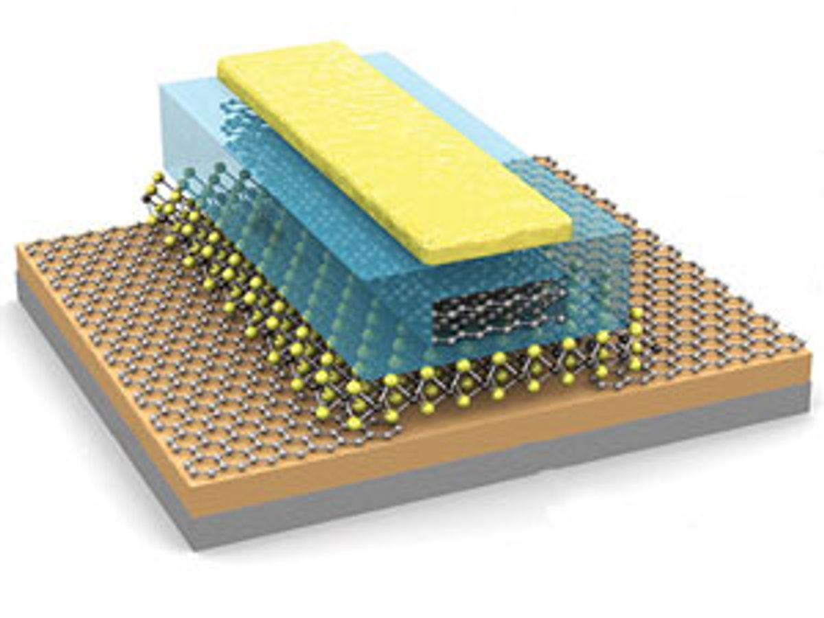
The flash memory prototype was built around field-effect geometry that forms the basis of field-effect transistors (FETs) used in complementary metal-oxide semiconductor (CMOS) electronics. In this case, the Swiss researchers replaced the silicon that would make up the middle layer of the sandwich-like device with the molybdenite. Graphene electrodes reside beneath this layer of molybdenite to transmit electricity into the molybdenite. The top layer of the device is several layers of graphene, which capture electrical charge and thereby stores memory.
The researchers believe this architecture should make for a more efficient flash memory design. The graphene is a much better at conducting electricity than silicon and the molybdenite is more sensitive to charge because it is far thinner than silicon.
This is all pretty early-stage at this point, so it's understandable that reports on this research seem to lack any discussion of its potential for commercialization. It’s not clear that marrying graphene and molybdenum will keep flash memory the king of the hill, but at a minimum, the king may have enlisted some new allies.
Dexter Johnson is a contributing editor at IEEE Spectrum, with a focus on nanotechnology.


