High-power radio-frequency electronics are a hot commodity, both figuratively and literally. The transistors needed to amplify 5G and future 6G signals are struggling to handle the thermal load, causing a bottleneck in development. Engineers in the United States and England have teamed up to demonstrate a promising solution—swaddling individual transistors in a blanket of thermally conductive diamond to keep them cool.
“Thermal issues are currently one of the biggest bottlenecks that are plaguing any kind of microelectronics,” says team lead Srabanti Chowdhury, professor of electrical engineering at Stanford University. “We asked ourselves, ‘Can we perform device cooling at the very material level without paying a penalty in electrical performance?’”
Indeed, they could. The engineers grew a heat-wicking diamond layer right on top of individual transistors—their hottest points—as well as on their sides. Heat flowed through the diamond to a heat sink on the back of the device. With this technique, the researchers achieved temperatures 100 degrees Celsius lower without any degradation of the device’s electrical properties. They will report their findings in San Francisco at the IEEE International Electron Device Meeting in December.
They demonstrated their technique on gallium nitride (GaN) high-electron-mobility transistors, or HEMTs. GaN is the go-to alternative to silicon for high-frequency applications, as it can sustain higher electric fields and responds more quickly to electric field changes. GaN also breaks down at a higher temperature than silicon. But not high enough: “If you go by the physics of the material, you see what its potential is, and we’re nowhere close to that today,” says Chowdhury. Keeping GaN HEMTs cool as devices shrink and frequencies grow will allow them to live up to their physics-promised potential.
Keeping the transistors cool will allow them to deliver higher power at higher frequencies while keeping them small enough to power the next generation of radar, 6G, and more.
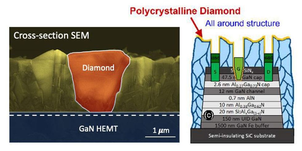 Engineers grew diamond crystals all around gallium nitride transistors to wick away heat at the source.Srabanti Chowdhury/Stanford
Chowdhury’s team’s approach is a stark departure from the common practice of bonding a heat sink to the whole chip on its back side. To bring a heat sink to the device level without adding unwanted capacitance that could slow a transistor down, Chowdhury and collaborators had to grow their polycrystalline diamond as a thin film with the smallest possible number of boundaries between different crystal grains. They also had to ensure that those boundaries had low thermal resistivity. Depositing diamond like that in a way that’s compatible with semiconductor foundry processors was an unlikely feat.
“Diamonds are universally the best thermal conductor,” says Mike Burkland, senior principal systems engineer at Raytheon Missile & Defense, who was not involved in the research. “The problem with conventional methods of diamond growth is that it requires high temperatures and high pressures. So, the real innovation that’s come out is being able to grow large enough diamond grains at low temperatures and low pressures for heat transfer from GaN devices. I wasn’t putting a lot of odds on this research being very successful just from difficulties in this in the past, but it was a tremendous job.”
The work was a large-scale collaboration between five universities. The particular type of HEMT used in the diamond growth was developed at the University of California, Santa Barbara, by Umesh Mishra’s research group. Samuel Graham’s team, first at Georgia Tech and then at the University of Maryland, performed stress management and stability testing. Mohamadali Malakoutian, a postdoctoral researcher in Chowdhury’s group, demonstrated the feasibility of low-temperature diamond growth. The thermal properties of the materials were then measured by Marin Kuball’s team at the University of Bristol. The all-around diamond, conceptualized by Chowdhury, was successfully put into practice by her group at Stanford, where Malakoutian and postdoc Rohith Soman built the HEMT, integrated the diamond, and measured the channel temperature to show the efficacy.
The next step will be transferring the technology out of the lab and into the industrial realm. These transistors have been manufactured for many years, and amending the process to add a new layer will not be easy. The new process will have to go through reliability testing and engineering for high yield. Chowdhury says her team is working with several industry partners on these issues.
The researchers also hope to bring the technique to other devices and semiconductor materials. “We are very excited that we are trying to bring this beyond gallium nitride,” Chowdhury says. “Really, our target is to make this a much more robust and a much more versatile platform for all semiconductors.”
Even if this remains a single semiconductor technique, the potential implications of beating GaN’s thermal issues are enormous. “The future of 5G or 6G is extremely dependent on gallium nitride HEMTs,” Chowdhury says. GaN transistors also could play a role in electric-vehicle charging and other applications that handle a lot of power in a small space. “When you make things compact, you produce more heat per unit area. If we’re prepared to deal with the heat, then all these innovations can go hand in hand and allow the solution to live up to its potential.”
Raytheon’s Burkland echoed this sentiment from his perspective as an industrial consumer of such devices. “I know myself and many others have been watching this research,” he says. “We’re really excited about it.”