
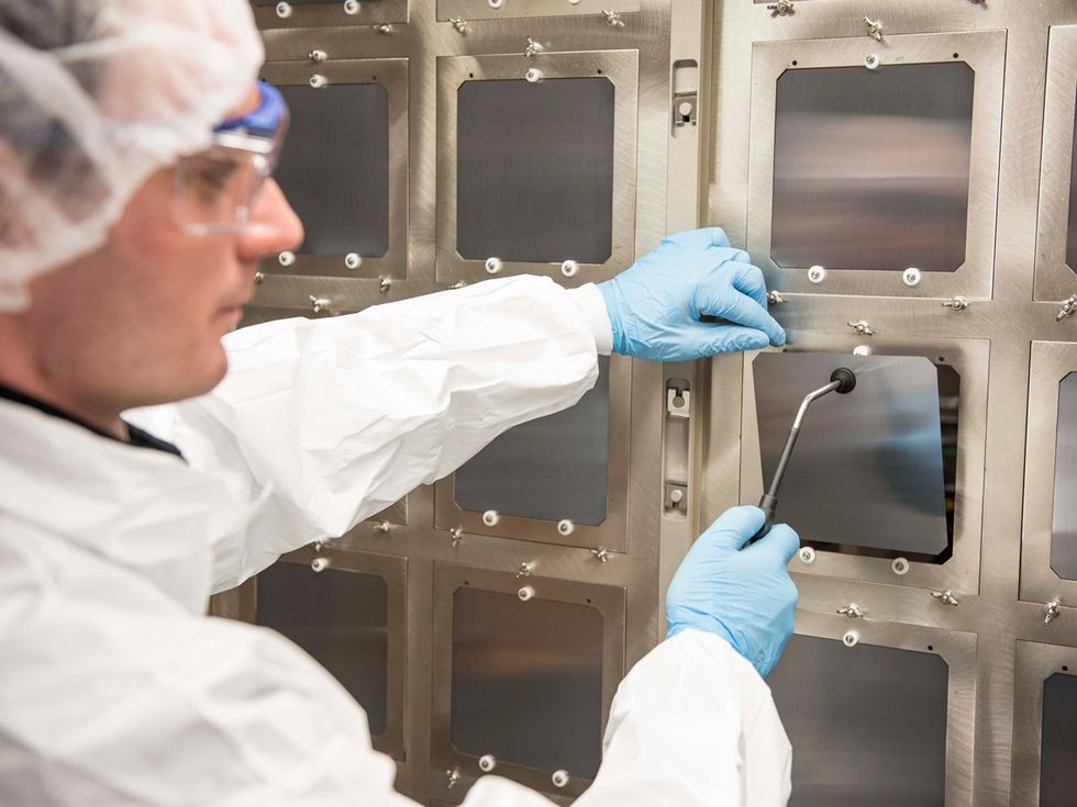
At a factory on the outskirts of Brandenburg en der Havel, Germany, bunny-suited technicians are manufacturing the future. The shiny, thin squares they’re assembling into flat modules promise to outperform the best solar panels on the market.
The pilot factory is owned by Oxford PV—a spinout from the University of Oxford, in England—which since 2012 has worked on commercializing solar cells made from a type of crystal known as a perovskite. The first perovskite solar cells were announced just 10 years ago, by the research team of Tsutomu Miyasaka at Toin University, in Yokohama, Japan. But those early lab prototypes were incredibly unstable and had an efficiency of just 3.8 percent.
Since then, researchers and manufacturers have made steep gains in efficiency, and they’ve also addressed the devices’ stability and scalability. In December, for example, Oxford PV posted its latest efficiency milestone of 28 percent. By contrast, the current record for silicon PV is 26.7 percent, and commercial silicon panels are far less efficient.
Now the company is getting ready to introduce the world’s first commercial tandem silicon-perovskite solar modules, which combine a thin-film layer of perovskite material with a silicon solar device. The solar modules look and behave very much like traditional silicon solar panels, says Chris Case, Oxford PV’s chief technology officer. The main difference is that they produce more power.
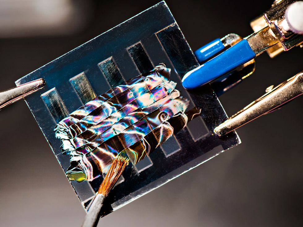
 Top This: In December, Oxford PV announced that its tandem perovskite-silicon solar cells had achieved 28 percent efficiency.Photo: Oxford PV
What makes these developments so remarkable is that just seven years ago, the perovskite solar industry didn’t even exist. Now, dozens of firms are vying to bring the technology to market. And hundreds of researchers worldwide are studying new perovskite materials and processing methods and refining their understanding of how the devices work. At press time, the number of academic papers on perovskites was on track to top 5,000 for 2018, Case says (although that number also includes reports on perovskites as photodetectors, X-ray detectors, and LEDs).
And in just 10 years, perovskites have gone from fussy, low-efficiency experimental devices to commercial-grade products that meet or exceed the performance of conventional solar cells. No other solar PV technology—not OLEDs, dye-sensitized or quantum-dot solar cells—compares.
“We’re at a disruption point in history,” Case says. “Right now, in most places in the world, solar PV without subsidies is cheaper than any other form of electrical generation.” Perovskites will ensure solar power’s conquest, he says.
“You can’t stop it. You can be the largest oil company in the world, but you can’t stop this.”
What makes perovskites so attractive is that the materials are much better than silicon at converting photons into electricity.
“One of my colleagues likes to say that if you were looking for the ideal material for solar, you would never pick silicon,” says Joseph Berry, who leads the perovskite solar team at the National Renewable Energy Laboratory (NREL), in Golden, Colo. “The reason [silicon] has become such a dominant material has everything to do with the total R&D dollars that have been spent on silicon,” for integrated circuits as well as solar.
“Silicon has to be pure and perfect to have the characteristics we covet,” Berry says. “Perovskites are defect tolerant. We can handle the material poorly and still get a competitive device efficiency.” Perovskites also lend themselves to a variety of low-cost production methods, including spin coating and roll-to-roll printing. NREL researchers have even developed a perovskite ink that can be painted on.
Berry predicts that constructing a gigawatt-scale factory for perovskite solar modules will eventually cost about a tenth of what it now costs to build a comparable silicon solar panel factory. The end product can be flexible and nearly transparent, so experts envision using them as window glazing and as spray-on coatings for buildings.
Perovskite originally referred to a mineral containing calcium, titanium, and oxygen, first discovered in 1839. The word has since come to encompass a large class of compounds that have the same crystal structure as the mineral. Their chemical composition is described by the shorthand AMX3, where A is typically an organic molecule, M is a metal (such as lead or tin), and X is a halogen (such as iodine or chlorine). Miyasaka’s group, at Toin University, used the compound methyl ammonium lead triiodide for its first perovskite cell. But there are hundreds of thousands of compounds that can form that crystal structure, according to Oxford PV’s Case.
Regardless of the chemistry, any perovskite solar cell has to meet three basic criteria for commercialization: stability, efficiency, and scalability. Case says his company has addressed all three by combining thin films of silicon and a perovskite into one “tandem” cell that can be produced using the same manufacturing methods used for today’s solar panels.
Back in 2012, when the company began working on perovskites, Oxford PV targeted pure-perovskite products that could be coated on glass and used as windows and other components of buildings. “That’s still a great idea, but we realized that the path to commercialization could be 5 to 10 years,” Case says. “We’re focused on delivering on a shorter horizon.”
When sunlight enters Oxford PV’s tandem cell, photons pass through a transparent electrode layer and then hit the perovskite layer, which absorbs at shorter wavelengths than silicon does, toward the blue end of the spectrum. The photons that aren’t absorbed then pass through a thin junction layer and encounter the silicon layer, which absorbs at somewhat longer wavelengths. The net result is that more of the available light is absorbed by the cell.
“To make a tandem cell that’s 26 or even 30 percent efficient, you only need a perovskite layer that’s in the range of 15 to 17 percent, plus a normal silicon layer that’s 20 percent efficient,” Case explains.
Oxford PV is far from alone in pursuing tandem perovskites. Other players include Toshiba and Panasonic in Japan and the Stanford spin-off Tandem PV. Meanwhile, a number of companies continue to bet on pure-perovskite solar cells: Poland’s Saule Technologies, China’s Wonder Solar and Microquanta Semiconductor, and the U.S. startup Energy Materials Corp. (EMC).
EMC didn’t set out to be a perovskite solar company. “Initially, we were based in Atlanta, developing something called optical antennas, which are a different way to convert light into electricity,” says EMC cofounder and CEO Stephan DeLuca. About three years ago, he says, “we realized that the path to commercialization was going to be long.” At that point, EMC switched to solar perovskites.
The startup’s focus is on commercializing roll-to-roll processing for its perovskite cells. “If you want to make these things low cost to compete with silicon, you have to do it fast,” DeLuca says. “Our target is to use a 1.5-meter-wide roll running at 50 meters a minute. That’s the kind of speed you need to scale up.”
Using vacuum deposition, as Oxford PV and other companies are doing, means “you need to cook the film for half an hour, so scaling up is more challenging,” DeLuca claims. Building a perovskite solar factory based on roll-to-roll processing should be significantly cheaper than one based on traditional silicon technology, he adds.
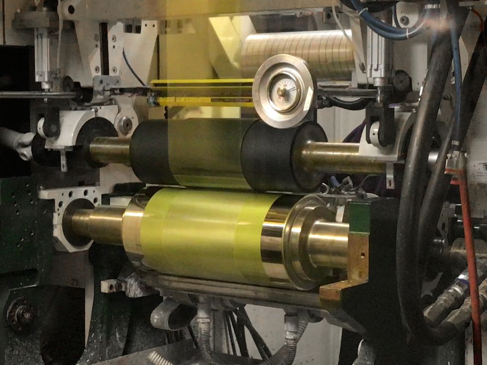
A couple of years ago, EMC relocated to Rochester, N.Y., to take advantage of the contract manufacturing facilities offered by Eastman Kodak. At present, EMC’s devices have five layers, which the roll-to-roll machine lays out in one pass.
EMC’s perovskite cells are based on a device architecture developed by Jinsong Huang and his team at the University of North Carolina at Chapel Hill. “Most people in this field use what’s called a NIP structure,” Huang says, referring to a device in which a layer of negatively doped (or n-type) material sits on top, with a layer of undoped “intrinsic” material in the middle and positively doped (or p-type) material at the bottom. One downside to NIP structures is that they require manufacturing temperatures of about 200 °C, which adds to their cost and limits the methods that can be used to make them.
EMC’s devices are PIN structures, with p-type material on top. “We find they work much better and can be fabricated using room-temperature processes,” including roll-to-roll printing. “It’s definitely the fastest approach you can think of,” Huang says. “There are already so many providers to make things like polymer thin films. You don’t have to reinvent every piece of equipment.”
Despite the enormous gains and intense activity, though, some solar researchers remain skeptical about the potential of perovskites. In a recent interview for PV Magazine, the Australian solar pioneer Martin Green noted that “there are all kind of instabilities that must be addressed,” including sensitivity to moisture, oxygen, and even light.
“It is very hard to see a silicon manufacturer adopting a product that is more efficient but doesn’t have the same stability as its baseline product—because no manufacturer wants to get a bad reputation regarding stability; in fact, it could be fatal,” Green was quoted as saying.
EMC’s DeLuca says that not all perovskites have that flaw. “The reporting of instabilities in certain perovskite formulations and device stacks has been important to the understanding of the materials but has also resulted in a misconception that perovskites as a class of materials all act the same—that is, they are all unstable,” says DeLuca. The misconception may spring in part from the fact that methyl ammonium lead triiodide, which is still widely used by academic researchers, is one of the unstable compounds. “The right choice of the perovskite material and the other layers making up the device stack yields stable devices.”
Case says that Oxford PV’s cells have been engineered to be stable and have passed every major accelerated lifetime test used for standard PV modules. The company will field the first modules in 2019, and it’s working with an as-yet-unnamed “major manufacturer of silicon solar cells and modules.”
In September, the company launched a £5 million (US $6.4 million) five-year joint research program with the University of Oxford aimed at reaching 37 percent efficiency. If the program succeeds, the result will be solar modules with nearly twice the power-converting ability of today’s commodity panels. And even if Oxford PV doesn’t hit that mark, another company probably will.
For his part, NREL’s Berry says it’s important not to rush the technology by bringing products to market that haven’t been fully vetted.
“When we started, I wasn’t a true believer,” Berry says. “I was of the opinion that if there’s a fatal flaw, let’s kill it and move on. Four years in, I think there is a real opportunity for this technology to change the world. That’s not an opportunity you get every day, and you certainly don’t want to mess it up.”
This article appears in the January 2019 print issue as “Perovskite Solar Cells: Ready for Prime Time.”