Terahertz spectroscopy uses infrared light to probe matter and is widely used to investigate the electrical properties and behavior of semiconductor materials. By sending very short laser pulses, called probe pulses, in quick succession, it is possible to follow how these properties change over time when the material responds to a light pulse, for example. However, unlike x-rays, terahertz waves have relatively long wavelengths ranging from 3 to 3000 micrometers. And just as with optical microscopes, structures smaller than the pulses’ wavelength remain invisible.
Now researchers at the University of Regensburg in Germany have demonstrated that it is possible to dramatically increase the spatial resolution of terahertz spectroscopy by focusing the probe pulses on the needle of an atomic force microscope (AFM). They published this research in Nature Photonics yesterday.
AFMs are widely used tools in solid-state research. Scanning with the sharp tip of the AFM at a slight distance from the surface of a material and measuring the variation of the force between the tip and the material—which can be an electrostatic or van der Waals force, for example—allows the creation of an image of the surface in which individual atoms are visible.
But the Regensburg researchers took a different tack. Instead of measuring the force between the tip and the surface of the material, they measured the intensity of light scattered by the tip with a series of probe pulses. According to Rupert Huber, the physicist who led the research, this method, “Is a little like a conventional radio antenna, just downscaled to wavelengths of infrared radiation.”
The light pulse, which is an oscillating electromagnetic field, shifts electrons up and down along the shaft of the metallic tip. However, because the electrons cannot travel beyond the tip, they accumulate at the very tip apex during each half cycle of the oscillating electromagnetic field. Since electrons are charged, they give rise to an intense burst light at the tip a very small area, called the near field, with roughly the size of the tip apex, explains Huber.
This setup, which the Regensburg team is calling a scattering-type near-field scanning optical microscope, or s-NSOM, confines light to an area that is only 10 nanometers across. Without the needle, one would be limited to about half the wavelength of the light, the diffraction limit that curtails the resolution of every conventional microscope. "In contrast, the near-field occupies a volume that is approximately nine orders of magnitude smaller than the usual diffraction limit,” Huber told IEEE Spectrum.
For their experiment, the Regensburg team used indium arsenide nanowires prepared by a group—who are coauthors of the Nature Photonics paper—at the Pisa site of CNRNano, a nanoscience institute of the Italian Research Council. Indium arsenide is a semiconducting material holding a promise for terahertz sources and infrared lasers.
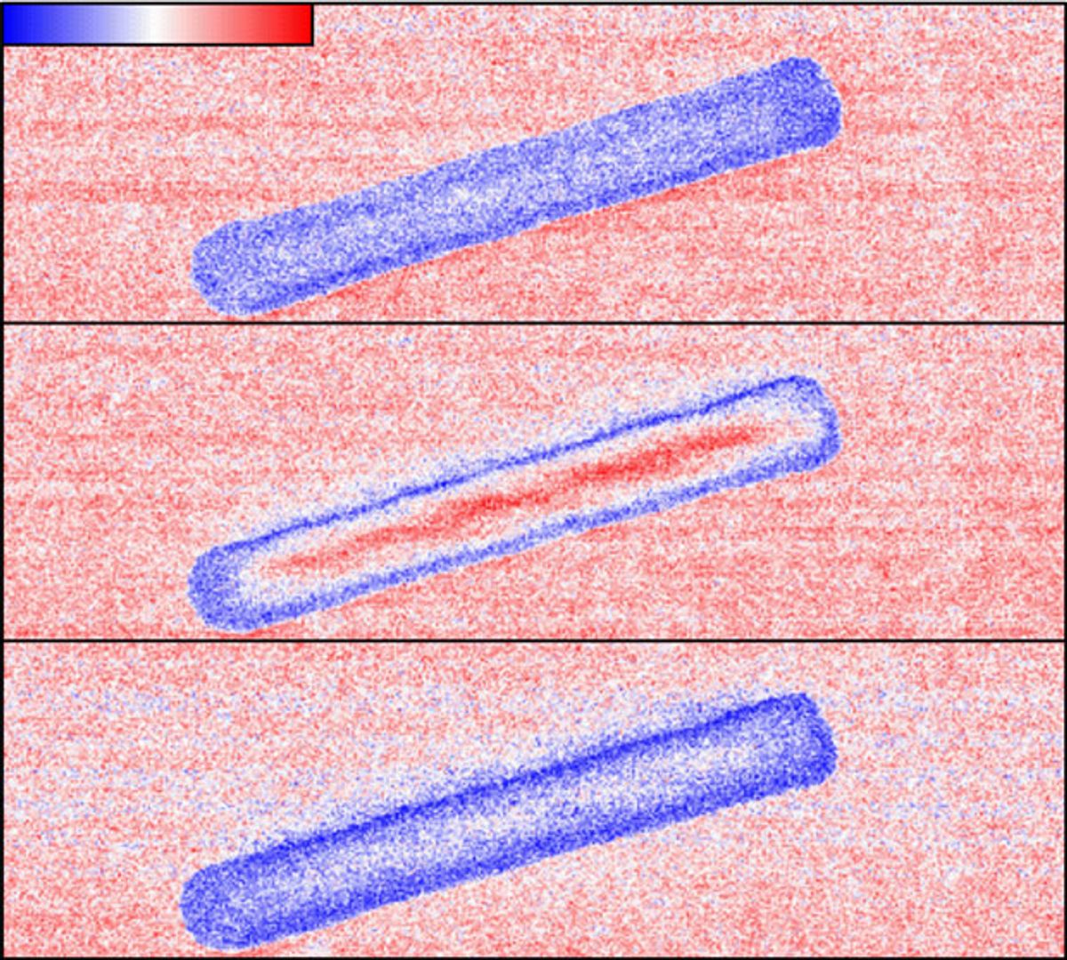
They first hit the nanotube with a terahertz pump pulse, which caused the liberation of charge carriers in the nanowire. This allowed them to detect the presence of electrons moving at the surface of nanowire—a little like what you would see if you disturb an ants' nest. Immediately after the pump pulse, they sent a series of terahertz probe pulses lasting few femtoseconds each. The pulses produced the 10-nm flashes of confined light on the tip. The intensity of these flashes depends on how many electrons are roaming around on the surface of the nanowire. These electrons don't stay around long, however; so, for every new probe pulse, the intensity of scattered light by the tip decreases.
By moving the tip to a new location for each pump cycle, the researchers created a complete "film" of how the nanowire reacts to the pump pulse. Among the phenomena they documented was that the free electrons first disappeared at the ends of the nanowires.
There is no reliable alternative, as of now, for measuring local carrier densities on the few-femtosecond time scale with 10-nm resolution, says Huber. "It is extremely important to understand how carriers behave locally. This insight is crucial for future high-speed integrated electronics and lasers based on semiconductor nanowires," he adds.


